Intel's Process Roadmap to 2025: with 4nm, 3nm, 20A and 18A?!
by Dr. Ian Cutress on July 26, 2021 5:00 PM ESTSidebar on Intel EUV
In all of these announcements, one thing to highlight is Intel mentioning its relationship with ASML, the sole company that manufactures the EUV machines powering production of leading edge semiconductor manufacturing.
ASML is a unique company in that it is the only one that can produce these machines, because the technology behind them is often tied up with its partners and research, but also because all the major silicon manufacturers are heavily invested in ASML. For any other company to compete against ASML would require building a separate network of expertise, a decade of innovation and design, and a lot of capital. None of the major silicon vendors want to disturb this balance and go off on their own, lest it shuts them out of the latest manufacturing technology, and no research fund sees competing against the embedded norm as a viable opportunity. This means that anyone wanting EUV specialist technology has to go to ASML.
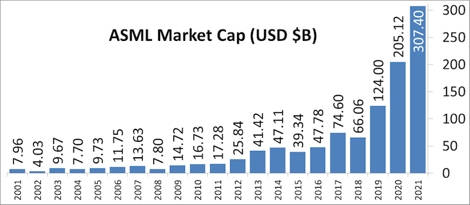
In 2012, it was reported that Intel, Samsung, and TSMC all invested in ASML. This was, at the time, to jumpstart EUV development along with migrating from 300mm wafers to 450mm wafers. While we haven’t moved to 450mm wafers yet (and there are doubts we will any time in the next decade), EUV is now here. Intel’s 2012 investment of $2.1 billion gave them a 10% stake in ASML, with Intel stating that it would continue investing up to a 25% stack. Those stakes are now below the 5% reporting threshold, but all three of the major foundry customers are still big owners, especially as ASML’s market cap has risen from $24 Billion in 2012 to $268 Billion in 2021 (surpassing Intel).
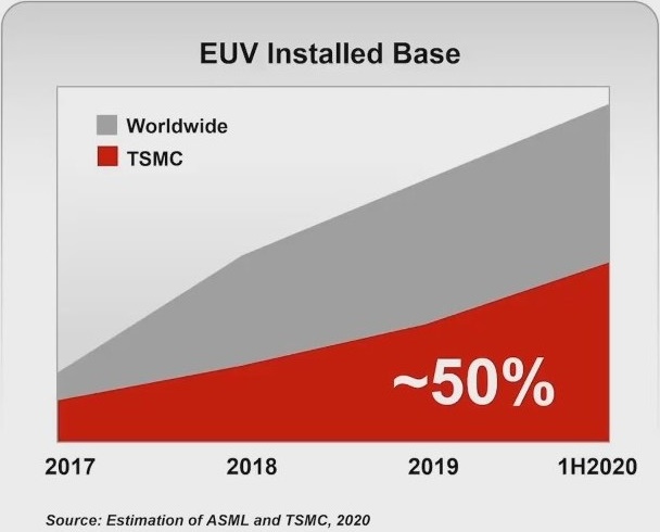
As major investors but also ASML’s customers, the race has been on for these foundries to acquire enough EUV machines to meet demand. TSMC reported in August 2020 that it has 50% of all EUV machines manufactured at ASML for its leading edge processes. Intel is a little behind, especially as none of Intel’s products in the market yet use any EUV. EUV will only intercept Intel’s portfolio with its new Intel 4 process, where it will be used extensively, mostly on the BEOL. But Intel still has to order machines when they need them, especially as there are reports that ASML currently has backorders of 50 EUV machines. In 2021, ASML is expected to manufacture around 45-50 machines, and 50-60 in 2022. The exact number of machines Intel has right now, or has ordered from ASML, is unknown. It is expected that each one has a ~$150m price tag, and can take 4-6 months to install.
With all that being said, Intel’s discussion point today is that it will be the lead customer for ASML’s next generation EUV technology known as High-NA EUV. NA in this context relates to the ‘numerical aperture’ of the EUV machine, or to put simply, how wide you can make the EUV beam inside the machine before it hits the wafer. The wider the beam before you hit the wafer, the more intense it can be when it hits the wafer, which increases how accurately the lines are printed. Normally in lithography to get better printed lines, we move from single patterning to double patterning (or quad patterning) to get that effect, which decreases yield. The move to High-NA would mean that the ecosystem can stay on single patterning for longer, which some have quoted as allowing the industry to ‘stay aligned with Moore’s Law longer’.
| ASML's EUV Shipments | |||||||||||||||||||||
| 2015 | 2016 | 2017 | 2018 | 2019 | 2020 | 2021 | |||||||||||||||
| Actual | 2 | 4 | 10 | 3 | 4 | 5 | 6 | 4 | 7 | 7 | 8 | 4 | 7 | 14 | 8 | 7 | 9 | - | - | ||
| Target (Total) | - | - | - | 20 (18) | 30 (26) | 35 (33) | 45-50 | ||||||||||||||
| 2018 and beyond is split per quarter for actual shipped numbers Data taken from ASML's Financial Reports |
|||||||||||||||||||||
Current EUV systems are NA 0.33, while the new systems are NA 0.55. ASML’s latest update suggests that it expects customers to be using High-NA for production in 2025/2026, which means that Intel is likely going to be getting the first machine (ASML NXE:5000 we think) in mid-2024. Exactly how many High-NA machines ASML intends to produce in that time frame is unknown, as if they flood the market, having the first won’t be a big win. However if there is a slow High-NA ramp, it will be up to Intel to capitalize on its advantage.


326 Comments
View All Comments
yannigr2 - Tuesday, July 27, 2021 - link
This is probably the only site on the Internet that swallows Intel's marketing and puts(on the title) "3nm" next to Intel's name.I would expect better from this site.
I guess Intel is hiring.
mode_13h - Tuesday, July 27, 2021 - link
Good point. Even Intel doesn't call it "3 nm". They call it "Intel 3". The title shouldn't misrepresent what they're actually saying.zodiacfml - Tuesday, July 27, 2021 - link
i agree. can't believe theyre just eating all this crap whereas they could have easily investigated Intel's 10nm 8 core laptop vs. AMD/TSMC 7nm laptop chips.29a - Tuesday, July 27, 2021 - link
It's become quite the shitshow since Anand sold the site, I'm only now realizing he sold it to FoxNews.ET - Tuesday, July 27, 2021 - link
It's certainly an aggressive roadmap. I'll be waiting to see how it turns out.mode_13h - Tuesday, July 27, 2021 - link
Intel's process roadmaps have never lacked in ambition.Timoo - Tuesday, July 27, 2021 - link
Ah, you have to firgive them. They simply didn't understand yet that the slave boats with 2 whipmen and hundreds of rowers have been "out of fashion" for quite some time now.siuba - Tuesday, July 27, 2021 - link
intel 7nm (intel 4) ... the table information incorrect.. it should be 200MTr/mm2+.. 5/4nm (Intel 3) density still unknown..Gondalf - Tuesday, July 27, 2021 - link
Looking at the suboptimal density found in Apple A14 SOC (5nm TSMC), this look like a good roadmap. We must remember that TSMC does a lot of claims about great density, still we find disappointing results in final products.There is too much enphasis on density, a lot less on availability of the process across the customers and a lot less about real yields at the claimed high density.
Bet in these days many have pissed off TSMC (Automotive, Nvidia in primis). A lot of claims but in pratics TSMC can not satisfy the demand cause low yields, simple and plain. AMD is a good example of the disaster. Qualcomm large utilization of Samsung say a lot.
name99 - Tuesday, July 27, 2021 - link
This statement about TSMC is a strong claim. The ONLY validated TSMC 5 density we have is A14/M1 and those are weird cases bcs Apple’s ONLY priority with them was to ship on time and working correctly (as far as x86/Mac transition matters). Physical optimization may have been tossed overboard as schedule slipped.There are claims that the Huaiwei chip fabbed on N5 met TSMC density as expected, but since few have seen that chip (bcs US forced Huawei off TSMC) who knows?
I’d wait for an alternative chip on N5 (should be one soon, surely) before making strong density claims.