Semiconductors
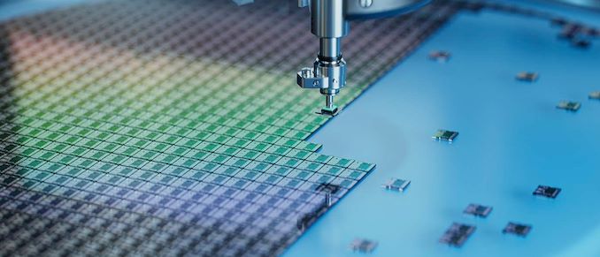
One of the core challenges that Rapidus will face when it kicks off volume production of chips on its 2nm-class process technology in 2027 is lining up customers. With Intel, Samsung, and TSMC all slated to offer their own 2nm-class nodes by that time, Rapidus will need some kind of advantage to attract customers away from its more established rivals. To that end, the company thinks they've found their edge: fully automated packaging that will allow for shorter chip lead times than manned packaging operations. In an interview with Nikkei, Rapidus' president, Atsuyoshi Koike, outlined the company's vision to use advanced packaging as a competitive edge for the new fab. The Hokkaido facility, which is currently under construction and is expecting to begin equipment installation...
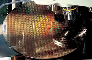
TSMC Details 3nm Process Technology: Full Node Scaling for 2H22 Volume Production
At TSMC’s annual Technology Symposium, the Taiwanese semiconductor manufacturer detailed characteristics of its future 3nm process node as well as laying out a roadmap for 5nm successors in the...
58 by Andrei Frumusanu on 8/24/2020Marvell Unveils its Comprehensive Custom ASIC Offering
Last week Marvell had updated us with an overview of the company’s new more extensive and comprehensive custom ASIC offerings, detailing the company’s design abilities gained through the company's...
6 by Andrei Frumusanu on 7/27/2020
Altair Semiconductor Renames to Sony Semiconductor Israel
Today, after more than four years of being acquired by Sony, Altair Semiconductor is renaming itself as Sony Semiconductor Israel. The IoT focused company over the last few years...
4 by Andrei Frumusanu on 7/21/2020
Analog Devices To Buy Maxim Integrated
Today Analog Devices has announced that it will be acquiring Maxim Integrated in a transaction estimated at $21bn. The combined company value is said to end up being valued...
17 by Andrei Frumusanu on 7/13/2020
TSMC To Build 5nm Fab In Arizona, Set To Come Online In 2024
In a big shift to their manufacturing operations – and a big political win domestically – TSMC has announced that the company will be building a new, high-end fab...
100 by Ryan Smith on 5/15/2020
Samsung to Produce DDR5 in 2021 (with EUV)
Samsung is on track to start volume production of DDR5 and LPDDR5 memory next year using a manufacturing technology that will take advantage of extreme ultraviolet lithography (EUVL). In...
20 by Anton Shilov on 3/25/2020
SMIC Details Its N+1 Process Technology: 7nm Performance in China
SMIC first started volume production of chips using its 14 nm FinFET fabrication process in Q4 2019. Since then, the company has been hard at work developing its next...
20 by Anton Shilov on 3/23/2020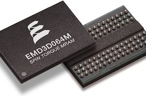
GlobalFoundries & Everspin Extend MRAM Pact to 12nm
GlobalFoundries and Everspin have announced that the two have extended their Spin-transfer Torque (STT-MRAM) joint development agreement (JDA) to 12LP (12 nm FinFET) platform. The extension will enable GlobalFoundries...
4 by Anton Shilov on 3/13/2020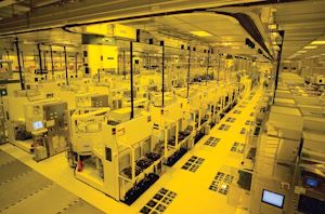
TSMC & Broadcom Develop 1,700 mm2 CoWoS Interposer: 2X Larger Than Reticles
With transistor shrinks slowing and demand for HPC gear growing, as of late there has been an increased interest in chip solutions larger than the reticle size of a...
18 by Anton Shilov on 3/4/2020
A Big Bet on SOI: GlobalFoundries Preps Another Supply Agreement for 300mm SOI Wafers
Having dropped out of the race for leading-edge manufacturing technologies in order to focus on specialty fabrication processes, GlobalFoundries has pinned some big hopes in manufacturing RF-SOI chips for...
26 by Anton Shilov on 2/27/2020
GlobalFoundries' 22FDX with MRAM is Ready
GlobalFoundries on Thursday said that it had completed development of its 22FDX (22 nm FD-SOI) technology with embedded magnetoresistive non-volatile memory (eMRAM). The technology can be used for a...
7 by Anton Shilov on 2/27/2020
Samsung Starts Mass Production at V1: A Dedicated EUV Fab for 7nm, 6nm, 5nm, 4nm, 3nm Nodes
Samsung Foundry has started mass production of chips using its 6LPP and 7LPP manufacturing processes at its new V1 fab. The new facility employs one of the industry’s first...
30 by Anton Shilov on 2/20/2020
ASML Ramps Up EUV Scanners Production: 35 in 2020, Up to 50 in 2021
ASML shipped 26 extreme ultraviolet lithography (EUVL) step-and-scan systems to its customers last year, and the company plans to increase shipments to around 35 in 2020. And the ramp-up...
22 by Anton Shilov on 1/23/2020
TSMC Boosts CapEx by $1 Billion, Expects N5 Node to Be Major Success
TSMC is on track to begin high-volume production of chips using its 5 nm technology in the coming months, the company said in its conference call last week. While...
40 by Anton Shilov on 1/22/2020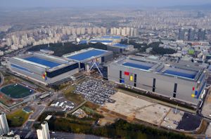
Samsung’s Fab in Hwaseong Suffers Power Outage
Samsung had to stop production of DRAM and V-NAND memory at its fab near Hwaseong, South Korea, due to power outage earlier this week. Damage caused by disruption of...
48 by Anton Shilov on 1/2/2020
Japan Partly Removes Restrictions on Photoresists Exports to South Korea
Marking a thawing of relations between the Japanese and South Korean governments, the Japanese Ministry of Economy, Trade and Industry (METI) has partially removed export restrictions on photoresists to...
16 by Anton Shilov on 12/23/2019
Intel Hires Fab Veteran, Former GlobalFoundries CTO Dr. Gary Patton
Intel has hired Dr. Gary Patton, the former CTO at GlobalFoundries and an ex-head of IBM Microelectronics business. Dr Patton was leading Global Foundries leading edge processes before that...
21 by Anton Shilov on 12/11/2019
Panasonic to Sell Semiconductor Business to Nuvoton
Panasonic has announced plans to almost completely withdraw from semiconductor business and sell all of its related assets to Taiwan-based Nuvoton Technology, a wholly owned subsidiary of Winbond Electronics...
6 by Anton Shilov on 11/29/2019
SMIC Begins Volume Production of 14 nm FinFET Chips: China’s First FinFET Line
SMIC has started volume production of chips using its 14 nm FinFET manufacturing technology. The largest contract maker of semiconductors in China is the first company in the country...
15 by Anton Shilov on 11/14/2019
GlobalFoundries and SiFive to Design HBM2E Implementation on 12LP/12LP+
GlobalFoundries and SiFive announced on Tuesday that they will be co-developing an implementation of HBM2E memory for GloFo's 12LP and 12LP+ FinFET process technologies. The IP package will enable...
13 by Anton Shilov on 11/5/2019


