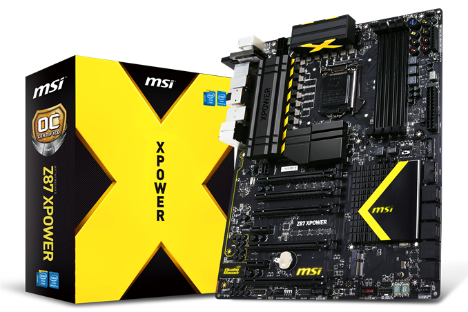
MSI Z87 XPower Review: Our First Z87 with PLX8747
by Ian Cutress on August 12, 2013 9:00 AM EST- Posted in
- Motherboards
- MSI
- PLX
- Z87
When it comes to motherboard extravagance, X58 heralded some mightily expensive boards, and a choice few from X79 and Z77 also raised this baton. So where does a $440 Z87 motherboard sit in this genre? Today we tackle the MSI Z87 XPower.
In the history of expensive consumer motherboards, the Gigabyte X58A-UD9 at $700 and the ASRock X79 Extreme11 at $600 MSRP are both models that spring to mind. Each of these attempts to justify the price point with features, goodies, and aspects of the product that may only cater to specific crowds (or rather make the item the ‘halo’ option, hoping that the positive results produce an influx of sales down the chain). It is also worth noting that these other motherboards were for generally expensive platforms to begin with. Admittedly the MSI Z87 XPower is quite below these price brackets, but the size, shape and target audience is not too distant from the older MSI X79 Big Bang XPower II, which was $390 at launch (and we gave it a silver award). Also in this price bracket worthy of note comes several ASUS ROG models from across over the years.
MSI Z87 XPower Overview
When I had previously seen the MSI ‘Power’ range of Z87 motherboards in press releases and at media events, it was a little perplexing to see the differences between them with a quick glance. Within the spectrum we have the MPower (the enthusiast motherboard), the XPower (the overclockers model) and the MPower MAX (a bridge between the two). All three, at quick glance, looked similar, with the larger heatsinks of the MPower MAX and XPower defining their position ahead of the MPower. Now when I actually got the XPower in for review, the first thing I noticed was the length of the motherboard, and instantly drew parallels to the MSI X79 Big Bang XPower II – this board has effectively nine PCIe slots of size. This limits the number of cases it can be fitted in, increases cost, but allows a good deal of wiggle room for routing, tracing, and features on the motherboard.
As a result, the XPower tries to hit the high notes that make all the PR numbers light up – a full fat 32 phase power delivery, the PLX8747 chip for four-way SLI, a PLX bypass for single GPU users, 802.11n WiFi (2x2:2 Centrino N-2230 which means 2.4 GHz), a Killer E2205 Gaming NIC, 10 SATA ports, two onboard USB 3.0 headers, 12 total USB 3.0 ports, the Realtek ALC1150 audio chip, goodies in the box and a three year warranty. It aims to be the halo board for the MSI range, and at $440 it has the price to match, although the 2.4 GHz WiFi is clearly not a halo solution and was not up to standard in my 2.4 GHz crowded apartment block.
After testing, several things become clear. The most positive stance on the box is that at stock speeds, the MSI Z87 XPower comes out as a well rounded board benchmark-wise. It is clearly designed for multi-GPU in a big way and wants to provide that efficiency, even if it means being a 9-slot motherboard.
It is however still in the early stages of development – the BIOS is not yet mature, even for reputable 24/7 use. The BIOS shipped with the board (1.1b4) had issues retaining XMP between boots, the latest public BIOS at the time of writing (1.0) enabled XMP but had stability issues, and the latest beta BIOS still requires a manual in order to learn to adjust all the OC settings. This is on top of an excruciatingly long POST time, which was 25 seconds with two GPUs POSTing to Windows 7 (this is in comparison to the best Z87 boards needing less than 10 seconds). Other issues that cannot be fixed overnight are the long traces from the audio codec to the rear IO audio, resulting in lower performance of the ALC1150 than some ALC898 solutions in both dynamic range and THD+N.
When the MSI Z87 XPower is stable and functioning the way you want/need it to, the motherboard does draw more power than the other Z87 motherboards we have tested due to the extra controllers and PLX chip used. For example the Z77X-UP7 had 32 phases and was in a similar position, compared to the motherboards that used <16 phases and were more power efficient than standard 8-phase ATX solutions.
$440 is a big ask from MSI, which is placated some by the inclusion of a mouse mat and goodies in the box, and from a design perspective the XPower does look the part. However the BIOS needs to mature/ultimately be more stable (which will come in time), and I can imagine that reducing the power delivery to 16 phases then pushing that money into a 5 GHz WiFi solution would make this a better product for the casual user. The MPower and MPower MAX are $235 and $260 respectively, with the MPower being a 24/7 friendly and the MPower MAX geared for overclockers, suggesting that at just over half the price MSI has better options unless you (a) want MSI and (b) need 3xSLI and above with avenues to (c) sub-zero overclocking.
Visual Inspection
Two obvious things strike you as you pull the MSI Z87 XPower out of its box – the size of the motherboard, and the size of the power delivery heatsink. The motherboard comes in under the loosely defined E-ATX standard, meaning ‘bigger than ATX’ – in the case of the XPower, we are talking an extra inch on the bottom of the motherboard, much like the MSI X79 Big Bang XPower II covered last year. This allows for the full gamut of PCIe lanes for four-way and extra space for features.

The big heatsink for the power delivery is designed to cater for the 32-phase power delivery as well as the PLX8747 chip hiding between the CPU and the PCIe slots. MSI have put this power delivery on board, as well as two 8-pin CPU power connectors, to help competitive overclockers who may draw 600W+ while under extreme sub-zero temperatures. For daily use, arguably using this arrangement may result in less stress per power phase, reducing the likely of one going bad, although the failure rate is multiplied by the number of phases on board that could fail. I think this is a little bit of a misnomer, as I have never had a motherboard fail due to bad power phases in my daily builds, although if you combine MSI’s Military Class vision in the mix, stick this motherboard in a humid atmosphere running strong overclocks and the situation could be warranted.
The heatsink grows over what is typically the first PCIe slot, in order to cover the PLX8747 chip. We reported how the PLX8747 chip works while looking at similar Z77 motherboards, but to summarize, it uses a FIFO buffer and acts as a mux to supply 32 lanes to the PCIe slots from 16 on the CPU. This gives the MSI Z87 XPower access to 32 lanes, meaning x16/x16, x16/x8/x8 or x8/x8/x8/x8 Crossfire and SLI setups. MSI also put in a PCIe 3.0 x16 bypass slot in there, so single GPU users can get the full benefit of a direct x16 from the CPU rather than via a bridge chip.
However, moving back to the socket and I had no issues fitting my TRUE Copper CPU cooler to the XPower. For fan headers, the socket area has four within easy reach – two 4-pin CPU headers at the top right of the board, a 4-pin SYS to the bottom left of the power delivery heatsink, and a 4-pin SYS between the PLX chip and the memory slots. The other three fan headers are found such that one 4-pin SYS is on the bottom right of the board, one 4-pin SYS is next to the CeaseFire switches at the bottom of the board, and the final 4-pin SYS is next to the first PCIe x1 slot on the left.
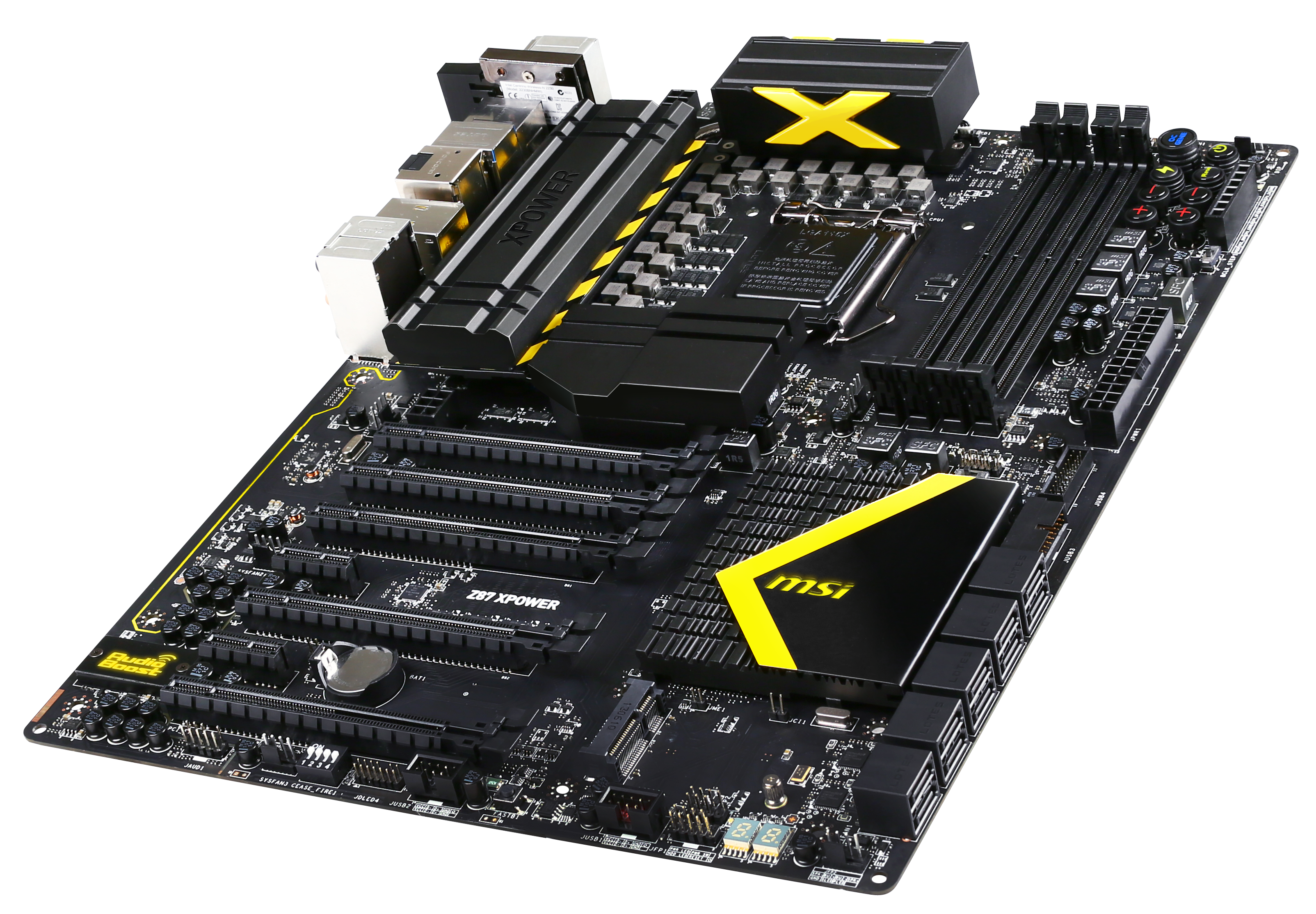
Moving clockwise around the motherboard from the CPU socket, and the memory slots come in double-latched black. On this size motherboard it does not particularly matter if the memory slots are double or single latched – the distance to the first PCIe slot gives plenty of room to place and remove memory in an overclocking scenario, but single slot latches are always preferred (in my point of view).
At the top right of the board we have the overclocking buttons:
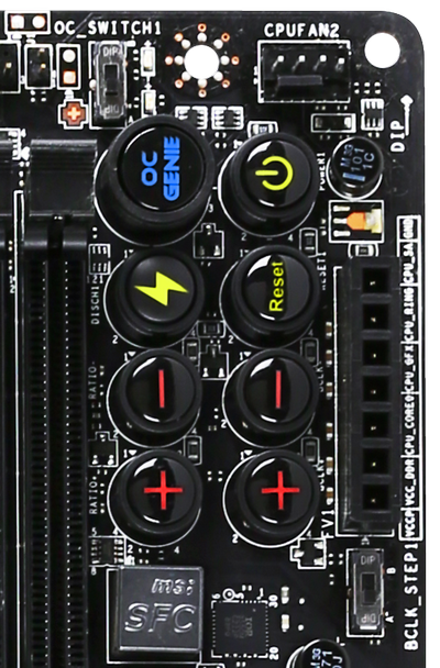
Firstly we get the OC Genie, a long-term characteristic of MSI motherboards for the one button instant overclock. This has a second ratio switch just above it labelled ‘OC_SWITCH1’ which controls either an easy overclock (4770K to 4.0 GHz) or a stronger overclock (4770K to 4.2 GHz). The power/reset buttons are obvious enough, but something new to the system is the Discharge button, represented by the lightning bolt. This button has a great function – it dissipates all energy from the system, causing it to shut down and the BIOS to reset. It is thus the ultimate kill switch without breaking anything, and in terms of OC buttons onboard is a nice addition – the only downside is that it is the same size and shape as all the other buttons, meaning when accidentally pressed all the BIOS settings go out of the window.
The final four buttons with +/- motifs on are to do with on-the-fly CPU speed adjustments. The plus and minus buttons nearest the memory deal with CPU Multiplier Ratio, and the other buttons deal with BCLK. These final two also have a DIP switch which controls the level of granularity on board – either 1 MHz or 0.1 MHz. Alongside all these are our V-Check points, to allow overclockers to monitor voltages without relying on software interpretations.
As we move down the right hand side of the motherboard, over the 24-pin ATX power connector, we have a MultiBIOS switch for selecting between the two BIOS chips on board, and two USB 3.0 headers, with one header at right angles so not to interfere with any full length PCIe devices. Both of these USB headers are powered by the chipset, relegating those on the rear IO to USB 3.0 controllers.
The chipset heatsink is relatively large, although from the board layout it looks like it deals with the chipset plus a few switches. It does not cover the two extra SATA 6 Gbps controllers for example, which are found to the bottom right of the heatsink next to their respective ports. We get 10 SATA 6 Gbps in total – six from the chipset and four from the controllers. MSI have also added an mSATA port, which shares allocation with the SATA5 port, meaning only one or the other can be used at any one time.
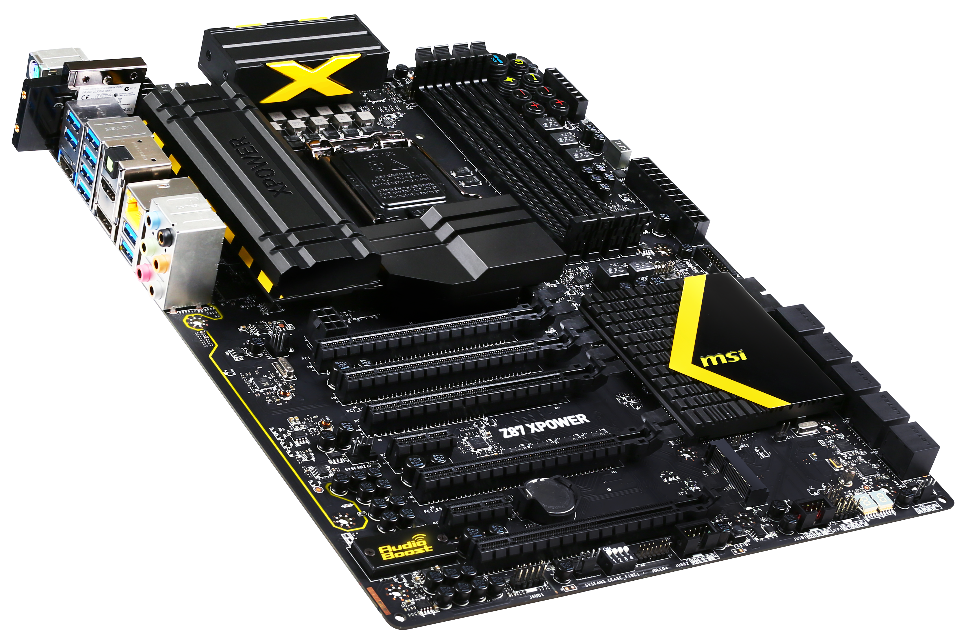
Along the bottom of the board, from left to right, we first get our audio solution. This is MSI’s Audio Boost, which uses the Realtek ALC1150 audio codec and the front panel audio gets additional headphone amps to support 600 ohm headphones. Due to the size of the motherboard, this means that the tracing for the rear panel audio travels a fair distance to the audio jacks. This is perhaps one reason our audio results on the rear IO are not necessarily the best for an ALC1150 implementation.
Continuing along the bottom of the Z87 XPower we get fan headers, CeaseFire (DIP switches to enable/disable PCIe slots), two USB 2.0 headers, the Go2BIOS button and our two digit debug. I use features like Go2BIOS a lot when overclocking, although this button would be better served either with the OC buttons on the top right of the motherboard or on the rear IO above the ClearCMOS button.
The PCIe layout attempts to take full advantage of the PLX chip, and PCIe 1/3/5/7 come from the PLX such that we get x16/x16 (1/5), x8/x8/x16 (1/3/5) or x8/x8/x8/x8 when all are occupied. PCIe 2 is an x16 slot that bypasses the PLX chip, giving a small boost to single GPU users as the PLX would add a nominal reduction in performance (<0.5%). I had a thought while testing this board as these bypass lanes are getting more common – could we bypass the PLX into x8/x8 on the same motherboard? The difference between x8/x8 via CPU and x16/x16 via the PLX in our testing is about as equivalent as single GPU x16 via CPU and x16 via PLX is.
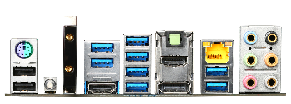
On the rear IO panel we get a PS/2 combination port, two USB 2.0 ports, a ClearCMOS button, integrated 2x2:2 2.4 GHz 802.11n (Centrino N-2230) WiFi, eight USB 3.0 ports (all ASMedia), two HDMI, DisplayPort, the Killer E2205 NIC and gold plated audio jacks.
Board Features
| MSI Z87 XPower | |||||||
| Price | Link | ||||||
| Size | E-ATX | ||||||
| CPU Interface | LGA-1150 | ||||||
| Chipset | Intel Z87 | ||||||
| Memory Slots |
Four DDR3 DIMM slots supporting up to 32 GB Up to Dual Channel, 1066-3000 MHz |
||||||
| Video Outputs |
2 x HDMI DisplayPort |
||||||
| Onboard LAN | Killer E2205 | ||||||
| Onboard Audio | Audio Boost (Realtek ALC1150) | ||||||
| Expansion Slots |
1 x PCIe 3.0 via CPU (x16) 4 x PCIe 3.0 via PLX8747 (x16/x16, x16/x8/x8 or x8/x8x/8/x8) 2 x PCIe 2.0 x1 |
||||||
| Onboard SATA/RAID |
6 x SATA 6 Gbps (PCH), RAID 0, 1, 5, 10 4 x SATA 6 Gbps (ASMedia ASM1061) 1 x mSATA 6 Gbps* *mSATA and SATA5 port share resources and using one disables the other |
||||||
| USB 3.0 |
4 x USB 3.0 (PCH) [2 headers] 8 x USB 3.0 (ASMedia ASM1074) [8 back panel] |
||||||
|
Flex IO x+y+z = 18 |
|
||||||
| Onboard |
10 x SATA 6 Gbps 2 x USB 3.0 Headers 2 x USB 2.0 Headers 7 x Fan Headers Discharge Button OC Genie Button BCLK Adjusters CPU Ratio Adjusters MultiBIOS Switch Go2BIOS Button Power/Reset Buttons PCIe Ceasefire Switches Two Digit Debug LED 14x V-Check Points (7 connectors, 7 spots) |
||||||
| Power Connectors |
1 x 24-pin ATX Power Connector 2 x 8-pin CPU Power Connectors 1 x 6-pin VGA Power Connector |
||||||
| Fan Headers |
2 x CPU (4-pin) 5 x SYS (4-pin) |
||||||
| IO Panel |
1 x PS/2 Combination Port 2 x USB 2.0 Ports 1 x ClearCMOS Button 1 x WiFi/BT Module Connector 8 x USB 3.0 Ports (ASMedia ASM1074) 2 x HDMI 1 x DisplayPOrt 1 x Killer E2205 NIC Audio Jacks |
||||||
| Warranty Period | 3 Years | ||||||
| Product Page | Link | ||||||
A PLX8747 chip, for those that buy it in bulk, stretch the materials cost by at most $40, though motherboard vendors that produce a lot of PLX enabled boards might get this cost down a fair chunk. MSI only make one PLX Z87 motherboard, the XPower, meaning that they might be nearer the $40 mark.
In terms of extra hardware, having 10 SATA ports and 14 total USB 3.0 ports would seem to be standard for a $440 motherboard, however at this price I would have expected at least a better WiFi solution than 2.4 GHz 2x2:2. Would it break the bank to get the 5 GHz model? For Z87 motherboards around $220 we are getting 802.11ac 5 GHz on MSI’s competitors, so it seems that someone has just decided to tick the WiFi box without doing some research into the ideal silicon, and saved a dollar here or there. Not only this, as shown later in the review, there is also an argument of no Intel NIC onboard, regardless of using the Killer solution.
The XPower is that odd mix of an overclocking and a daily use motherboard, but unfortunately does neither to the best it could be. There might be too much fluff for a true overclocking platform, and too many unused extras for a daily machine, to be able to justify the cost to the end-user. This puts us back into the realm of the MPower and MPower MAX, as mentioned in the introduction.


35 Comments
View All Comments
DanNeely - Monday, August 12, 2013 - link
I'm wondering about the pair of USB2 ports on the back. The Z87 provides 6 USB3 ports; 4 are used by the pair of onboard headers, and all 8 back panel USB3 ports are ASmedia. This leaves 2 USB3 ports on the z87 idle, so why not route them to the back too instead of USB2.IanCutress - Monday, August 12, 2013 - link
You are forgetting FlexIO (http://www.anandtech.com/show/6989/) - Z87 has 18 ports from the PCH. Most of them are fixed - four for USB 3.0, six for PCIe 2.0 and four for SATA 6 Gbps. This leaves two pairs of two - the first pair can be configured as USB 3.0 or PCIe 2.0, and the second pair can be configured as PCIe 2.0 or SATA 6 Gbps. The only limitation is a maximum of eight PCIe 2.0 lanes in total. MSI have decided to use four USB 3.0 here, eight PCIe 2.0 and six SATA 6 Gbps: 4 + 8 + 6 = 18, as shown in the Board Features :)Ian
ionR19 - Sunday, August 10, 2014 - link
there are 4 USB3 comming from the PCH and 8 from the hubscan you use all the 12 USB3 ports this way ?
BryanDobbins - Saturday, August 17, 2013 - link
On Saturday I got a gorgeous Ariel Atom after earning $6566 this – four weeks past, after lot of struggels Google,Yahoo,Facebook proffessionals have been revealed the way and cope with gape for increase home income in suffcient free time.You can make $85 an hour working from home easily.i m started from this link... http://goo.gl/4D5GN3
KurtToni - Monday, August 12, 2013 - link
Love my job, since I've been bringing in $82h… I sit at home, music playing while I work in front of my new iMac that I got now that I'm making it online. (Home more information)http://goo.gl/jhiOeM
tech6 - Monday, August 12, 2013 - link
In most home uses cases the bottleneck for performance is no longer the CPU but more likely to be the graphics card or hard disk. Thus spending a lot of money on on OC board is a waste of money better spent on an SSD or more GPU. I guess that manufacturers are betting that there will always be enough well funded fanbois who feel the need to brag about their OC numbers to make a buck on products such as these.IanCutress - Monday, August 12, 2013 - link
Overclocking, at least competitive overclocking, has substantial investment in motherboard companies and is the the focus of peoples jobs, careers, and a sport-like industry. The website HWBot.org is a common database for overclock scores and leagues, and I have reported here at AnandTech about competitive overclocking events/venues. Manufacturers will always release boards for these people, though it's hard to justify it *just* for this crowd, and it has to be made for daily use as well. As a result you end up with a Halo board trying to cater for both crowds, as mentioned in the conclusion ;)Ian
Slomo4shO - Monday, August 12, 2013 - link
Why don't any of these board manufactures ever design a board capable of 3-way crossfire/SLI using PCIe 1, 4, and 7 slots? ASRock x79 boards are the only ones that seem to have this option currently...Infy2 - Monday, August 12, 2013 - link
What does that plus (+) mean in the performance charts next to the system name?IanCutress - Monday, August 12, 2013 - link
It means that the CPU was tested in a motherboard that enables MultiCore Turbo/Enhancement/Acceleration by default, like this one. It is starting to become the norm for motherboards from certain companies over a particular price point.Ian