TSMC Forms 3DFabric Alliance to Accelerate Development of 2.5D & 3D Chiplet Products
by Anton Shilov on October 27, 2022 1:15 PM EST- Posted in
- Semiconductors
- TSMC
- CoWoS
- SoIC
- InFO
Currently the majority of high-end processors are monolithic, but design methodologies are slowly but surely shifting to multi-chiplet modules as leading-edge fabrication technologies get more expensive to use. In the coming years multi-chiplet system-in-packages (SiPs) are expected to become much more widespread, and advanced 2.5D and 3D chip packaging technologies will gain importance. To accelerate and simplify development of 3D designs, TSMC this week established its 3DFabric Alliance.
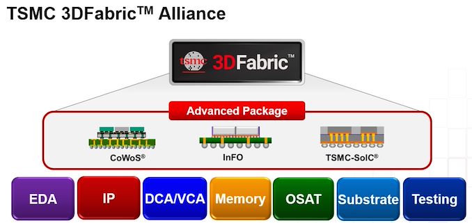
While multi-chiplet SiPs promise to simplify development and verification of highly complex designs, they require brand-new development methodologies as 3D packages bring a number of new challenges. This includes new design flows required for 3D integration, new methods of power delivery, new packaging technologies, and new testing techniques. To make the best use of the benefits of TSMC's 2.5D and 3D packaging technologies (InFO, CoWoS, and SoIC), the chip development industry needs the whole ecosystem to work in concert on chiplet packaging – and this is what 3DFabric Alliance is designed to do.
“3D silicon stacking and advanced packaging technologies open the door to a new era of chip-level and system-level innovation, and also require extensive ecosystem collaboration to help designers navigate the best path through the myriad options and approaches available to them,” said Dr. L.C. Lu, TSMC fellow and vice president of design and technology platform.
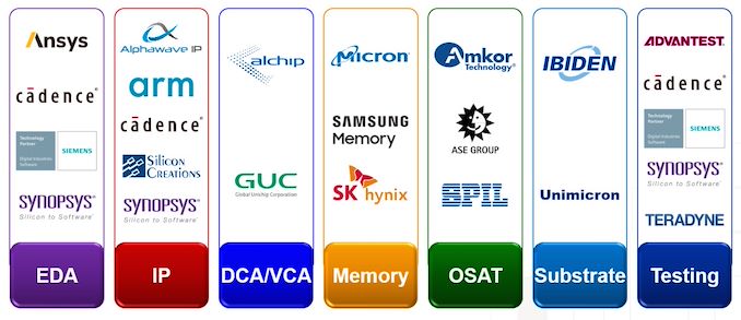
TSMC's 3DFabric Alliance brings together developers of electronic design automation (EDA) tools, intellectual property providers, contract chip designers, memory manufacturers, advanced substrate producers, semiconductor assembly and test companies, and the groups making the equipment used for testing and verification. The alliance currently has 19 members, but over time it is expected to expand as new members join the group.
As the leader of the Alliance, TSMC will set certain ground rules and standards. Meanwhile members of 3DFabric Alliance will co-define and co-develop some of the specifications for TSMC's 3DFabric technologies, will gain early access to TSMC's 3DFabric roadmap and specs to align their plans with the foundry's plans as well as those of other members of the alliance, and will be able to design and optimize solutions that are compatible with the new packaging methods.
Ultimately, TSMC wants to ensure that members of 3DFabric Alliance will offer its clients compatible and interoperable solutions that will enable quick development and verification of multi-chiplet SiPs that use 2.5D and 3D packaging.
For example, to unify the design ecosystem with qualified EDA tools and flows, TSMC has developed its 3Dblox standard. 3Dblox covers various aspects of building multi-chiplet devices featuring 2.5D and 3D packaging methodologies (such as chiplet and interface definitions), including physical implementation, power consumption, heat dissipation, electro-migration IR drop (EMIR), and timing/physical verification.
“Through the collective leadership of TSMC and our ecosystem partners, our 3DFabric Alliance offers customers an easy and flexible way to unlocking the power of 3D IC in their designs, and we can’t wait to see the innovations they can create with our 3DFabric technologies,” added Lu.
Ultimately, TSMC envisions that the alliance will greatly simplify and streamline the process for developing more advanced chips, especially for small and mid-size companies that rely more heavily on outside IP/designs. For example, if a company wants to develop a SiP consisting of logic chiplets stacked together and connected to an HBM3-based memory subsystem, EDA software from Ansys Cadence, Synopsys, and Siemens will allow it to design compatible chiplets, IP providers will sell those blocks the designer does not already have, TSMC will produce silicon, memory producers will offer compatible HBM3 KGSDs (known good stack dies), and then Ase Technology will assemble everything together. Meanwhile companies that do not have their own engineers will be able to order the design of the whole SiP (or individual chiplets) through Alchip or GUC, and then update their product over time if needed without needing to redesign everything, as the SiP will be built in accordance with 3DFabric and 3Dblox standards.
3Dblox is currently supported by four major EDA developers. Eventually it will be supported by all members of the members if the alliance where needed.
While large companies like AMD and Nvidia tend to develop their own IP, interconnection, and packaging technologies, multi-chiplet SiPs promise to make the development of complex, chiplet-style processors accessible to smaller companies. For them, standard third-party IP, fast time-to-market, and proper integration are key to success, so 3DFabric Alliance and what it brings will be vital for them.
Source: TSMC


9 Comments
View All Comments
Exotica - Thursday, October 27, 2022 - link
How does this 3DBlox initiative compare and/or compete with UCIe?thestryker - Thursday, October 27, 2022 - link
The way I read it 3DBlox should incorporate UCIe as it seems to have rather broad scope.Threska - Thursday, October 27, 2022 - link
Well Backside Power Delivery is what's really needed.https://www.fabricatedknowledge.com/p/backside-pow...
nandnandnand - Thursday, October 27, 2022 - link
It's supposed to lower power consumption, right? I didn't see that in the article or maybe I skimmed over it.Lakados - Saturday, October 29, 2022 - link
Is this TSMC trying to put together an alternative to Intels tiles?evanh - Tuesday, November 22, 2022 - link
Nope, this is TSMC generalising for regular contract work what was custom for AMD for the past four years.SiliconFly - Thursday, December 8, 2022 - link
It's actually TSMC trying to catch up with Intel. Just fyi, they've both been in this business for close to 3 to 4 decades. And Intel had always been the leader. In 2017, Intel lost footing and started doing the unpleasant 14+++ thing. Coupled with the 10nm delays, their foundry lost a total of 4 years doing nothing.Then came Pat Gelsinger.
He ditched the existing 7nm node. Added EUV & multi-patterning and turned it into a 4nm node. Intel 4nm is actually on par with current TSMC 3nm. And is already ahead of schedule by 6 months!
He then introduced Intel 3nm which is also ahead of schedule by 6 months and will be on par with the upcoming TSMC N3 variants (e/p/s/x).
And then, the most unexpected & unimaginable thing happened. Intel announced that it's 20A & 18A are also very much ahead of schedule! Meaning, Intel 2nm will volume ramp in 2024 while TSMC 2nm is expected to be production ready ONLY IN 2026! This is hard to believe but true.
I wouldn't be so sure of Intel 18A yield as it relies very heavily on multi-patterning for increase in MTr/mm2. Ring any bells? Might be a repeat of 10++++. That's why they've confined it to a niche product: A 15W LP cpu. Just a moonshot/sideshow. Might not make it on time.
In essence, they have now progressed much better than TSMC. EUV, Tiles, 3D Stacking, Disaggregated IP, GAA, BPD. The amount of progress made by Intel has TSMC worried already. But there's only so much tsmc can do. Their ROI is 3 years minimum i think for a new node running at full capacity. Cos, they have to have different types of nodes, libraries, etc to support all types of customers.
Intel on the other hand, Intel doesn't have that many generic nodes (except Intel 3). Most nodes are designed to service very specific needs. So, the nodes remain lean & mean & nimble and a lot cheaper than a comparable TSMC node. For an custom Intel node, the ROI is roughly half that of TSMC.
So, TSMC is now trying to catch up with Intel Innovation. Otherwise, starting 2024, TSMC will lose leadership is all aspects.
SarahKerrigan - Wednesday, December 14, 2022 - link
Hi Pat! How's the weather in Santa Clara?Zoolook - Monday, December 26, 2022 - link
LOL even Intels PR department couldn't come up with this, I think you should add an /s otherwise some people will think you are serious!