Xilinx Announces World Largest FPGA: Virtex Ultrascale+ VU19P with 9m Cells
by Dr. Ian Cutress on August 27, 2019 10:00 AM EST- Posted in
- FPGAs
- Xilinx
- Ultrascale
- VU19P
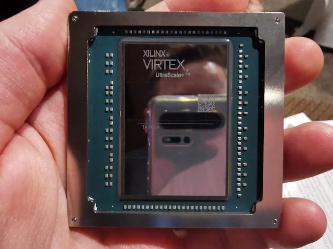
We don’t often cover the FPGA market here at AnandTech, but in the past couple of years we have seen the array of features that FPGAs are implementing expand at an incredible rate. Xilinx has been at some of the forefront of those innovations, with products such as Versal on 7nm and its Alveo family. One key part of Xilinx’s business is emulation and simulation, which requires large FPGAs to fit large designs onto - and the company recently lifted the lid on its latest creation, the Virtex Ultrascale+ VU19P. This new FPGA, when it comes to market, will hold the title of the World’s Largest FPGA.
Large FPGAs are Big Business
An FPGA, or Field Programmable Gate Array, is a bit of hardware that helps circuit designers do their job. An FPGA is so programmable that a user can design an integrated circuit on an FPGA before the design goes to market, and the engineer can see if the design works, and get rough estimates on performance and accuracy. For example, on the biggest FPGA today, Xilinx’s 22nm-based Virtex Ultrascale 440, an engineer can simulate 10 concurrent Arm Cortex A9 cores. With the new UltraScale+ VU19P, that same engineer can simulate 16 of the same cores, due to the 1.6x increase in logic gates. FPGAs also act as a base for the latest designs and technologies, with specific IO logic that can be built into current and future communication technologies. The idea of an FPGA makes it more configurable than a CPU, but that configuration can then be taken to a fab and made into an optimized chip for better performance and density. Ultimately in order to design a CPU, you need an FPGA.
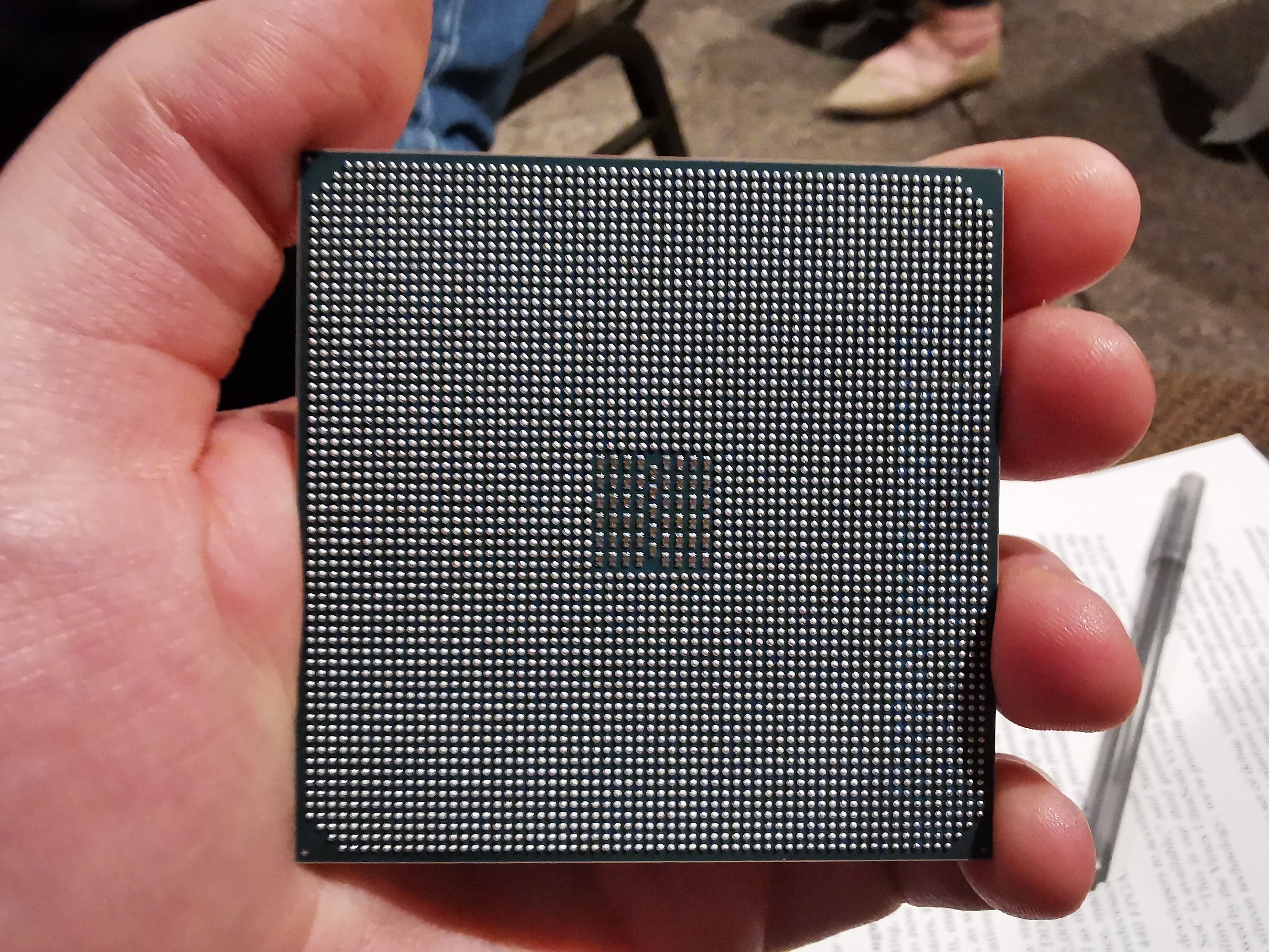
In the announcement, Xilinx explained that a sizeable part of its business is catering to this simulation and emulation market, used by all the chip vendors, and the drive to bigger chips gave them the impetus to create the VU19P. Built on TSMC’s 16FF+ process with CoWoS technology, the VU19P is actually built as four segments then placed on a die, however the chip acts as one seemless large piece of silicon, totaling 35 billion transistors. Along with the 9m logic gates, there is also over 2000 IO segments for 4.5 Terabits of transceiver bandwidth (80 lanes of 28G) and 1.5 Terabits of DDR4 memory bandwidth, which the company states will help its customers create designs featuring multiple VU19P chips in one system with all-to-all connectivity topology.
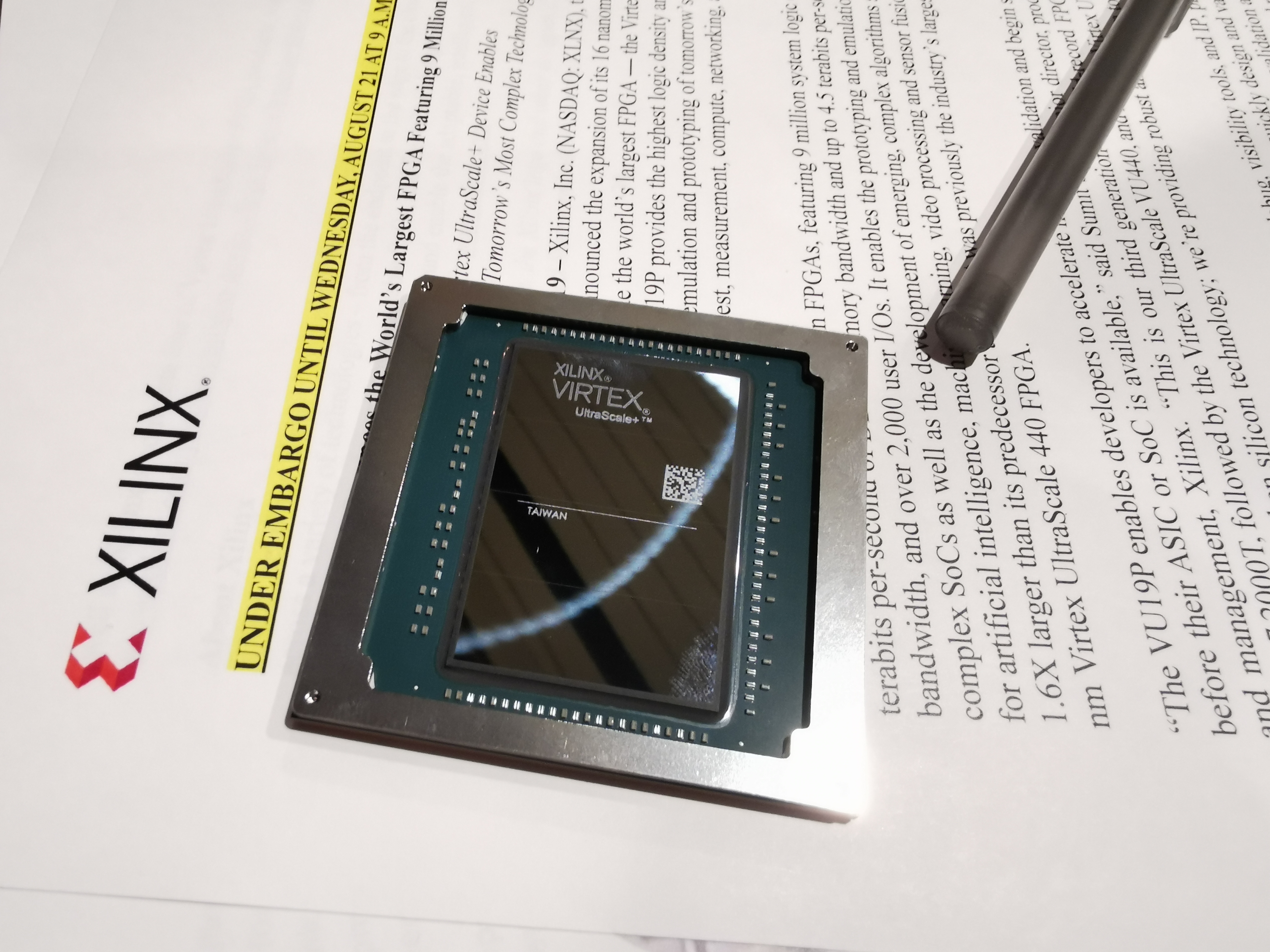
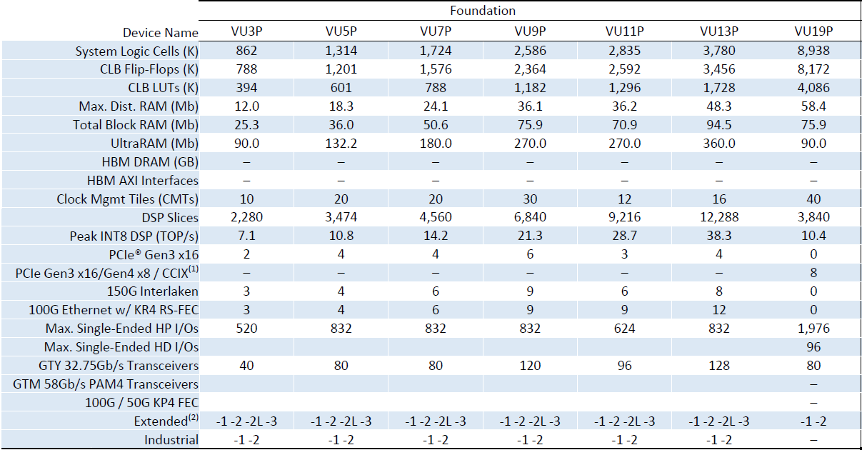
In PCIe card form the VU19P can be built as either a PCIe 3.0 x16 or PCIe 4.0 x8 device, or as a separate chip it can be used in a 65x65 package with a BGA3825 connection with the potential for CCIX connectivity. Other hardware features include 8.2m CLB Flip-Flops, 4.1m CLB LUTs, 90 Mb of UltraRAM, 40 Clock Management Tiles (CMTs), and 3840 DSP slices. Some of those numbers are quite a bit smaller than the UltraScale+ VU13P, which has only 4m logic gates, but this is due to the balancing of resources which Xilinx states will favor the simulation and emulation market.
Along with the VU19P, the company will also make enhancements to its Vivado Design Suite software to assist with co-optimization of the new chip. Xilinx is set to bring the VU19P to market in the fall of 2020 (~Q3), and will be ready to start sampling key partners in the first half of 2020.

I found a chip. It's @XilinxInc's new 'biggest FPGA ever', the Virtex Ultrascale+ VU19P with over 9 million logic cells, 35 billion transistors, and 80 x 28G IO. Built on TSMC 16FF+, coming in Q3 2020. pic.twitter.com/mn30mtenMY
— Dr. Ian Cutress (@IanCutress) August 21, 2019


17 Comments
View All Comments
Threska - Tuesday, August 27, 2019 - link
"The idea of an FPGA makes it more configurable than a CPU, but that configuration can then be taken to a fab and made into an optimized chip for better performance and density. "And speed. FPGAs have been limited in that area. The tools have also been rather proprietary to a given vendor.
MrSpadge - Wednesday, August 28, 2019 - link
I would say "speed" is included in "performance".ajp_anton - Tuesday, August 27, 2019 - link
You should change those "9m" and "4m" etc to capital M's. I kept reading to find out what these 9-meter and 4-meter cells are, but apparently (still not sure) the m somehow means millions.The Chill Blueberry - Tuesday, August 27, 2019 - link
It's millions of logic cells.. Whatever those are.mlkj - Tuesday, August 27, 2019 - link
Logic cells are a purely virtual marketing number, the meaningful number is the LUT6 and flipflop count.They invented LCs to show that not all LUTs are the same, but the Logic cell/LUT ratio is just an arbitrary multiplier (that they've apparently bumped to 2.1 for some inscrutable reason. It used to be 1.4, then ~1.6).
eastcoast_pete - Tuesday, August 27, 2019 - link
Thanks Ian! Impressive indeed, but I fear it's quite out of my price range. Did they say how much it is? Also, while you mention the ability of a large FGPA to simulate a CPU like the A55, a major use of these is to allow people to prototype or even implement a custom ASIC without having to fab a custom ASIC. Can come in handy if the task is still in flux. For example, one could implement an AV1 encoder on an FPGA like this in hardware, which is likely much more efficient and faster than any software-based solution. Also, might allow a deep learning system to optimize itself also in hardware, which could be an approach to beat even that ginormous Cerebras chip .Samus - Tuesday, August 27, 2019 - link
Yeah....This is probably like a $10,000 chip.Andy Chow - Tuesday, September 3, 2019 - link
Just look at nVidia's g-sync. To my knowledge, their still using an FGPA, because making a custom ASIC would not be cost-efficient. So often a large FGPA, while much slower than an ASIC, can completely remove the need to fab an ASIC depending on the volume you have to manufacture.From my perspective, I wish we will get more and more of these at consumer price, to emulate old hardware.
TokyoQuaSar - Wednesday, September 25, 2019 - link
For the price it depends on the quantity and the provider. One of the most expensive provider route is convenience retailers such as DigiKey who usually sell devices in small quantities for testing purposes mostly. In DigiKey the entry price for a VU440 in $36000. A VU13P costs at least $45000 and can go up to $80000 depending on the package used (IO capabilites etc) and speed/temperature grades.TokyoQuaSar - Wednesday, September 25, 2019 - link
About GSync I believe that at least the first versions were using an Altera FPGA, an Arria V GX iirc. It's not that expensive, definitely not something in the same world as the above mentionned FPGAs, but still not cheap enough (around $250 on Digikey, so maybe somewhere around $100 for mass prod.). I believe they could have used a Xilinx Artix-7 to do the same job, as I believe the limiting factor to use a cheaper device was the IO performance, and in terms of high speed transceiver vs cost, the Artix-7 does the best for video application imo (at least half the price of an Arria V GX). I guess the Artix 7 wasn't available yet when they did the design of the gsync module.