Toshiba Memory & Western Digital Finalize Fab K1 Investment Agreement
by Anton Shilov on May 20, 2019 9:00 AM EST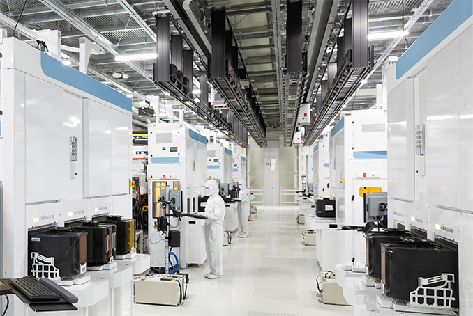
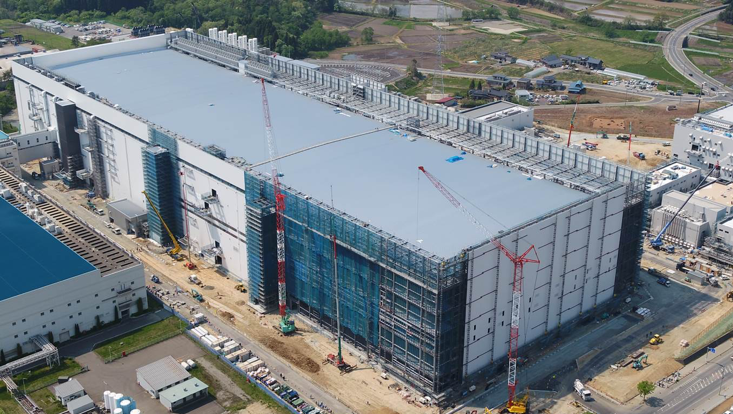
Toshiba Memory and Western Digital on Friday announced that they had finalized a formal agreement regarding a joint investment in the K1 manufacturing facility near Kitakami, Iwate Prefecture, Japan. The fab is currently being constructed by Toshiba Memory and is expected to come online next year, as planned.
New Fab and R&D Operations
The K1 building shell is being constructed in a single phase, while the cleanroom is being built over four similarly-sized phases. Equipment installation for a small initial production line in the Phase 1 of the cleanroom is set to begin in June 2019. When completed, the fab will be Toshiba Memory and Western Digital's largest manufacturing facility by size, and will also feature the greatest manufacturing capacity (because of the expanded cleanroom space). The first wafers – carrying 96-layer 3D NAND flash memory – will be produced at K1 in early 2020, with higher volume output expected in the second half of 2020.
In addition to building the fab, the two companies will also extend their joint R&D activities to the new site. At present, all of their R&D activity is conducted at a special technology development center near their jointly run Yokkaichi operations.
The Money
Under the terms of the agreement, Western Digital will fund 50% of the K1’s startup costs as well as 50% of the Phase 1 production line. The costs for the company, which include things like equipment investments, relocation costs, and startup costs will total about $660 million. Western Digital will also have to prepay around $360 million toward K1 building depreciation, which will take place over a three-year period starting in H2 2019.
As is usually the case with fabs jointly owned by Toshiba and Western Digital, the production facility will formally belong to a separate joint venture (in this case, Flash Forward Ltd., or FFL) that will sell wafers processed by the factory to its owners at cost. As soon as Western Digital owns a certain stake in the joint venture, it will be eligible to buy a number of wafers at equal costs with Toshiba Memory. However, even if that stake falls below a threshold, Western Digital will be accountable for bearing permanent costs related to K1’s operations at that threshold.
More details about the agreement will be published by Western Digital on Form 10-K for the fiscal year ending June 28, 2019.
The Largest Fab
As noted above, K1 will be the largest fab operated by Toshiba Memory and Western Digital. The two companies already run five manufacturing facilities: Fab 2, Fab 5, and Fab 6 are used to make 3D NAND, whereas Fab 3 and Fab 4 serve different purposes.
| Toshiba Memory & Western Digital NAND Production Operations | |||
| Fab | Purpose | Site | |
| Fab 2 | 3D NAND | Yokkaichi Operations | |
| Fab 3 | Special Purpose | ||
| Fab 4 | Special Purpose | ||
| Fab 5 | 3D NAND | ||
| Fab 6 | 3D NAND | ||
| Fab K1 | 3D NAND* | Kitakami Operations | |
| Note: | *Set to come online in 2020 | ||
The addition of K1 to Toshiba/WD's already formidable fleet of fabs will ultimately allow the company to continue scaling up their NAND flash capacity. So even with the current weakness in flash memory pricing, it appears that the two companies remain cautiously optimistic about the prospects for the flash market.

Related Reading:


1 Comments
View All Comments
A-Tech-fan-55 - Monday, May 20, 2019 - link
Any estimate for the predicted wafer/month target capacity for this fab?