ASML, Carl Zeiss, and Nikon to Settle Legal Disputes Over Immersion Lithography
by Anton Shilov on January 25, 2019 12:00 PM EST- Posted in
- Semiconductors
- Zeiss
- ASML
- DUV
- Nikon
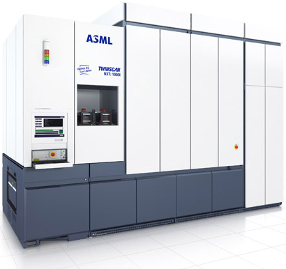
Embroiled for some time now in legal disputes concerning immersion lithography, ASML, Carl Zeiss, and Nikon, this week signed a memorandum of understanding relating to a plan to once again settle those disputes and give all parties full access to the technology. Under the terms of the deal, Nikon will get a one-time payment in cash, and the three companies will sign a cross-licensing agreement that contemplates mutual royalty payments for 10 years.
According to the yet-to-be-signed agreement, ASML and Zeiss will pay Nikon €150 million ($169.68 million) and then the three companies will pay each other royalty fees of 0.8% over the sales of immersion lithography tools for 10 years after the actual cross-licensing deal is signed. Meanwhile, the three companies will drop all pending charges between each other in all courts across the world (including the US ITC) and agree not to sue each other over immersion lithography (and digital cameras) during the period.
Back in 2017, ASML controlled a 85.4% share of the lithography tool market, Nikon had a 10.3% share, and Cannon commanded 4.3% of shipments, according to The Information Network. Given the current state of things on the market of semiconductor manufacturing equipment, the upcoming agreement would seem to be a clear win for Nikon, which will be getting rather hefty sums of money over the next decade without paying equal sums in return.
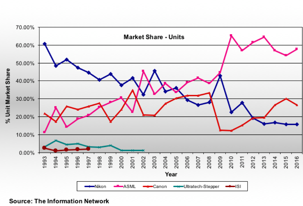
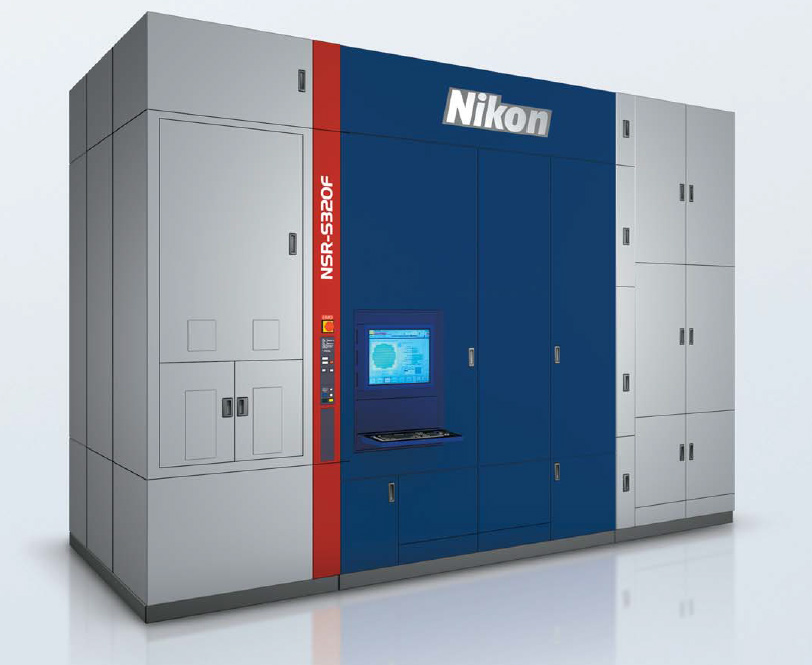
Even though they don't have ASML's current marketshare, Nikon was one of the semiconductor industry's pioneers with its lithography tools. As a result the company holds plenty of patents related to chip manufacturing equipment in general, and immersion lithography in particular. When the Japanese semiconductor industry was on its rise back in the 1980s and 1990s, Nikon controlled 50% – 60% of the lithography tools market in terms of units, whereas ASML merely commanded 12% – 25% of shipments, according to The Information Network. The situation began to change in the second half of the 1990s when American, Korean, and Taiwanese companies (AMD, Intel, Micron, Samsung, TSMC, UMC, etc.) served by ASML grew much stronger and so did their requirements for production equipment. ASML outsold Nikon in terms of units for the first time in 2002 and this is when its legal problems with the Japanese company began.
Nikon filed the first lawsuit against ASML and Zeiss (which supplies optics to ASML) accusing them of patent infringements in late 2001, then ASML accused Nikon of patent infringements in 2002. Since then, the two have been fighting both on the market and in the courtroom rather regularly. The two companies settled in 2004. ASML and Zeiss paid Nikon licensing fees till 2009, but then ceased. In 2017, Nikon sued ASML and its partner Zeiss again. ASML and Zeiss counter-sued Nikon in response.
This latest agreement means that after the companies sign their agreement next month, the trio of companies should once again be at relative peace for the next 10 years.
Related Reading:


6 Comments
View All Comments
Valantar - Saturday, January 26, 2019 - link
Hm. Wonder what, if any, effect this will have on lithography node shrinks going forward. I don't know much about this part of the industry, but ASML's near-monopoly can't be good for anyone wanting innovation, no matter how much their customers push them to improve their equipment. If there's only one company capable of delivering the most crucial equipment for producing every single high-end microchip in the world, that's rather scary.FullmetalTitan - Saturday, January 26, 2019 - link
This is exactly why the roll-out of EUV is so mixed across the top 3 players. There was a limit on available equipment because only ASML was making a viable platform for HVM in 2017/2018, with at most 1 unit delivered per month.Samsung bought the lion's share of the platforms in 2018, and only now are TSMC and Intel able to acquire the number of scanners needed to actually USE EUV in their processes.
Risk was certainly a consideration by all companies when deciding when to insert EUV, but there was just a hard supply limit as well.
source: colleague who went to work for ASML in 2017
Yojimbo - Saturday, January 26, 2019 - link
Other companies have tried different methods of achieving node shrinks. It's not like EUV was the only attempt, and even just 1 year ago you had people in these forums saying EUV wasn't going to work. 3 years ago you had people outside these forums saying EUV wasn't going to work.The development of EUV was subsidized by Intel, Samsung, etc. Intel chose not to employ EUV. They probably had the option before or alongside Samsung. Intel, however, expected their roadmap to look differently when they were making their decisions. It was less than 2 years ago, if I remember, when Intel was deciding on EUV use for their 7 nm node and and decided against it because they were worried it wouldn't be ready in time. I am sure they now wish they had made the opposite decision. They are adjusting to insert EUV. EUV wafers per hour and availability have improved faster than expected and Intel's nodes have been pushed back.
From the sound of it by ASML's CEO, what is holding back EUV tool production is the optics systems at Carl Zeiss. Perhaps it won't be much of an issue beyond 2019, though, because there are now only 3 foundries that are currently making the next-generation node shrink (after GlobalFoundries dropped out) and EUV isn't cost effective for memory, yet.
In any case, DUV is still usable, it just gets expensive. And DUV systems will be sold for a long time. ASML shares productivity increases from tools equally with their partners and that won't change because of a switch to EUV. ASML aren't not going to squeeze customers over EUV when it would end up costing them their DUV market. ASML also won't use EUV for pressure to get companies to adopt their DUV tools since ASML are already outcompeting their rivals in DUV anyway. If they start to do that then I am sure regulators will be quick to jump on board. I don't think it's scary.
frenchy_2001 - Tuesday, January 29, 2019 - link
EUV has been very long coming.ASML was the *only* company that took the risk and spent the money in R&D to develop it. They are now reaping the rewards. CANON and Nikon decided not to spend the ridiculous amount of money necessary to reach production level and only be secondary sources once the technology hit mainstream.
ASML almost died from that bet. They needed direct investment from all their possible customers (intel, TSMC, Samsung) to stay afloat during that period.
https://www.barrons.com/articles/intel-follows-sam...
Having a monopoly on a product is not against the law. It's abuse of that monopoly which is illegal.
So far, ASML has not abused their "power". They need their customers as much as they need ASML.