TechInsights Publishes Preliminary Analysis of 3D XPoint Memory
by Billy Tallis on May 27, 2017 8:01 AM EST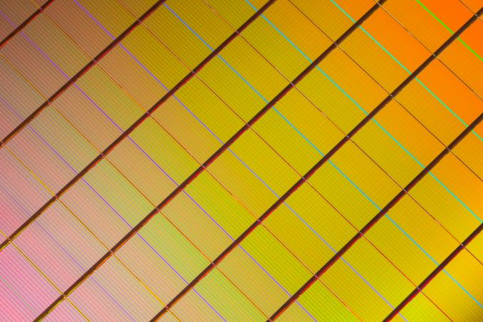
Now that the Intel Optane Memory M.2 SSDs are readily available on the open market, anyone with an electron microscope and the skills to use it can begin to probe the secrets of 3D XPoint memory that Intel and Micron have been keeping tightly under wraps since announcing the new technology in August 2015. The reverse engineering experts at TechInsights have been doing just that, and they recently published their initial findings.
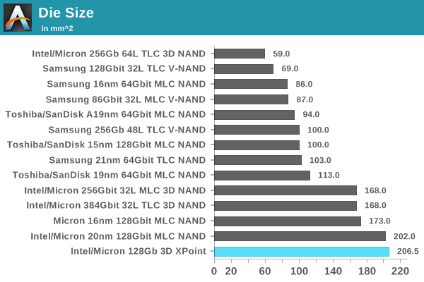
With some of the first high-resolution die photographs of 3D XPoint, TechInsights has provided precise measurements of the die size and memory density. The 128Gb 3D XPoint die is 206.5 mm2, much larger than is typical for modern NAND flash or DRAM but comparable to Intel's 128Gb 20nm planar MLC NAND. A large total die size is typical for Intel and Micron, as they have historically not catered to the mobile market with their NAND flash while competitors like Samsung and Toshiba have strived to ensure their flash will physically fit in devices like smartphones. (That trend is changing with the introduction this year of 64-layer 3D NAND where Intel and Micron are producing both a larger 512Gb TLC part and a smaller 256Gb TLC part.)
The Intel Optane SSD DC P4800X is using memory of similar density to the Intel SSD DC P3700 that it is displacing as the flagship of Intel's SSD product line. When comparing similar chips, die size is a strong predictor of manufacturing cost, but 3D XPoint memory is quite different from NAND flash memory, both older planar NAND or newer 3D NAND. Still, there's some value in noting that the P4800X is arriving with a price tag about 25% higher than the P3700 initially carried. This suggests that the manufacturing process for 3D XPoint is either more expensive than planar NAND or that 3D XPoint yields are not mature enough, but a lot of the markup can also be explained by the lack of high-performance competition for Optane SSDs.
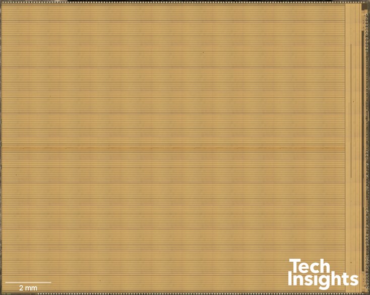
TechInsights calculates that 91.4% of the 3D XPoint die area is occupied by the memory array itself. This is a much higher figure than for NAND flash, where the record is 84.9% for Intel/Micron 3D NAND with its "CMOS under the array" design that puts a large portion of the peripheral circuitry underneath the memory array instead of alongside. Samsung's current 48-layer 3D V-NAND manages an array efficiency of just 70%, and 3D NAND from Toshiba and SK Hynix has been comparable. This means that once Intel gets around to increasing they layer count in future generations of 3D XPoint memory, they should be able to get much closer to the ideal capacity scaling than 3D NAND memory can currently achieve.
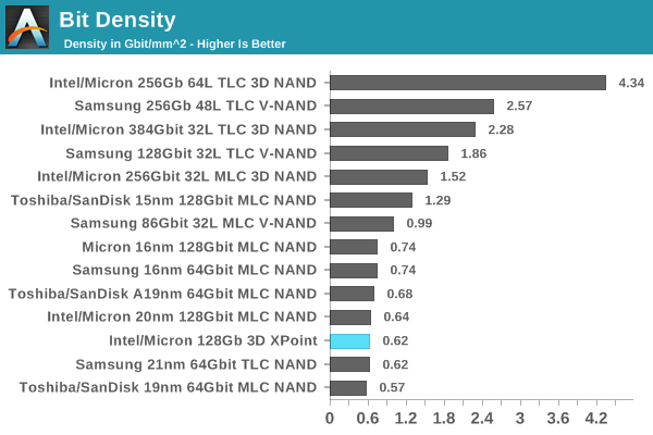
The analysis from TechInsights confirms that 3D XPoint memory is manufactured using a 20nm process, with the same pitch in both the bitline and wordline directions of the memory array. The DRAM market is only just moving beyond this milestone, so comparing the density of 3D XPoint to current DRAM highlights the fundamental capacity advantage 3D XPoint enjoys: around 4.5 times higher density compared to typical 20nm DRAM, and about 3.3 times higher than the most advanced 1Xnm DDR4 on the market. This gap is likely to widen with future generations of 3D XPoint.
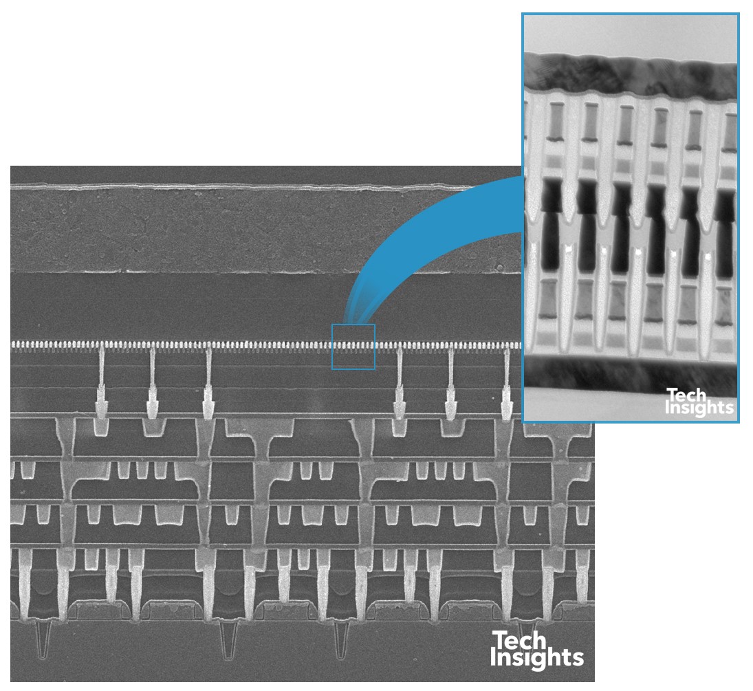
The materials and construction of an individual 3D XPoint memory cell have not been fully analyzed, but it appears to be a phase change memory element with a doped chalcogenide selector switch. The 3D XPoint memory array is constructed between the fourth and fifth metal interconnect layers above the silicon die.
Source: TechInsights


22 Comments
View All Comments
wumpus - Saturday, May 27, 2017 - link
Interesting article. I wonder if the emphasis on comparing 3dxpoint to MLC/TLC flash was techinsight's idea or anandtech's.From the original propaganda coming from Intel, I expected a memory that would barge in between DRAM and Flash, forcing DRAM to act more like a cache (presumably something like HBM connected to the CPU) and in turn caching slower, denser, and cheaper Flash (TLC or denser). This also appears to be what Intel thought with the shipping Optane, although that is pretty much moot after the introduction of pseudo-SLC 3d flash (no real caching needed, although it might make a good dram replacement in SSDs).
And of course the big questions remain: can Intel get the latency below milliseconds and get the endurance enough to use <1ms latency?
vladx - Saturday, May 27, 2017 - link
It's only the first generation, I think Intel's hype numbers were for much later when the technology finally matures.melgross - Saturday, May 27, 2017 - link
Seriously, I'm always surprised when tech types are disappointed in new technology. As it is, this provides a NJ get of major advantages, and it's just first generation. When did NAND first come out, 20 years ago? I still have a NAND card from my old Agfa minilab that cost US $250 and has 4MB storage (it was used to store settings in the machine.)Give this a few years. I mean, the first usable SSD was just 16GB. The ones we saw back then as really usable were, by todays standards for SSD, very slow, and cost $3,600 for a 32GB drive.
dwrivers - Saturday, May 27, 2017 - link
Take a look at the Optane drive review from a few weeks ago and you'll see that latency is <10uS with 5-9s <100uS. The endurance is listed as 30 drive-writes per day.Looks like the technology is delivering something new and exciting that fits between DRAM and NAND Flash.
http://www.anandtech.com/show/11209/intel-optane-s...
hahmed330 - Saturday, May 27, 2017 - link
Optane will probably never replace DRAM unless ridiculously drastic improvements are made since DRAM pretty much have a legendary endurance that optane probably could never match. As a caching scratch board it can make sense, but it's usefulness is quite limited especially for your average Joe.IntelUser2000 - Sunday, May 28, 2017 - link
You don't need it to completely replace DRAM. If the technology comes near to what they promised, then it can significantly reduce the need for DRAM. Right now the policy is to put much as possible into DRAM to mask slow speed of storage. When the storage is much faster, then it'll be different.But final goal for these devices won't be realized for 10-15 years. You need to overhaul the computer system from top to bottom. It's something that has been stable for 70 years, so, you are talking about mentality changes of the people involved in the low level computer architecture.
Revolution, comes as a stage. Never instant. Now the days of easy scaling is at an end, that'll be true even in semiconductors where traditionally newer device always offered better in every category.
melgross - Sunday, May 28, 2017 - link
Intel has never claimed that optane will completely replace RAM. You're setting up a straw argument that was never made, and then knocking it downBMNify - Sunday, May 28, 2017 - link
not really, as commercial Everspin Mram at 90nm is faster and can even now fit above the lower Dram for speed, then.. its also got a lot more nm room to grow and is already near infinite write Non-volatilityboeush - Saturday, May 27, 2017 - link
So they only need to stack 8 layers of this to leave the most advanced 3D NAND in the dust density/capacity-wise, without even stepping fien to a smaller process node. The only issue then would be cost per die - something that might well be resolved through higher volumes and better yields...I can see this completely replacing NAND within the next 10 years or so...
Kristian Vättö - Monday, May 29, 2017 - link
3D XPoint doesn't scale nearly as well as 3D NAND when it comes to layers. Cross-point arrays are built layer by layer, whereas 3D NAND has a vertical channel i.e. all layers are processed at once. PCM is also not that scalable when it comes to lithography because it too suffers from cell-to-cell interference.