New ARM IP Launched: CMN-600 Interconnect for 128 Cores and DMC-620, an 8Ch DDR4 IMC
by Johan De Gelas on September 27, 2016 11:00 AM EST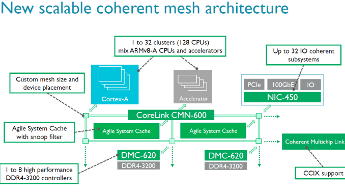
You need much more than a good CPU core to conquer the server world. As more cores are added, the way data moves from one part of the silicon to another gets more important. ARM has announced today a new and faster member to their SoC interconnect IP offerings in the form of CMN-600 (CMN stands for 'coherent mesh network', as opposed to cache coherent network of CCN). This is a direct update to CCN-500 series, which we've discussed at AnandTech before.
The idea behind a coherent mesh between cores as it stands in the ARM Server SoC space is that you can put a number of CPU clusters (e.g. four lots of 4xA53) and accelerators (custom or other IP) into one piece of silicon. Each part of the SoC has to work with everything else, and for that ARM offers a variety of interconnect licences for users who want to choose from ARM's IP range. For ARM licensees who pick multiple ARM parts, this makes it easier for to combine high core counts and accelerators in one large SoC.

The previous generation interconnect, the CCN-512, could support 12 clusters of 4 cores and maintain coherency, allowing for large 48-core chips. The new CMN-600 can support up to 128 cores (32 clusters of 4). As part of the announcement, There is also an agile system cache which a way for I/O devices to allocate memory and cache lines directly into the L3, reducing the latency of I/O without having to touch the core.
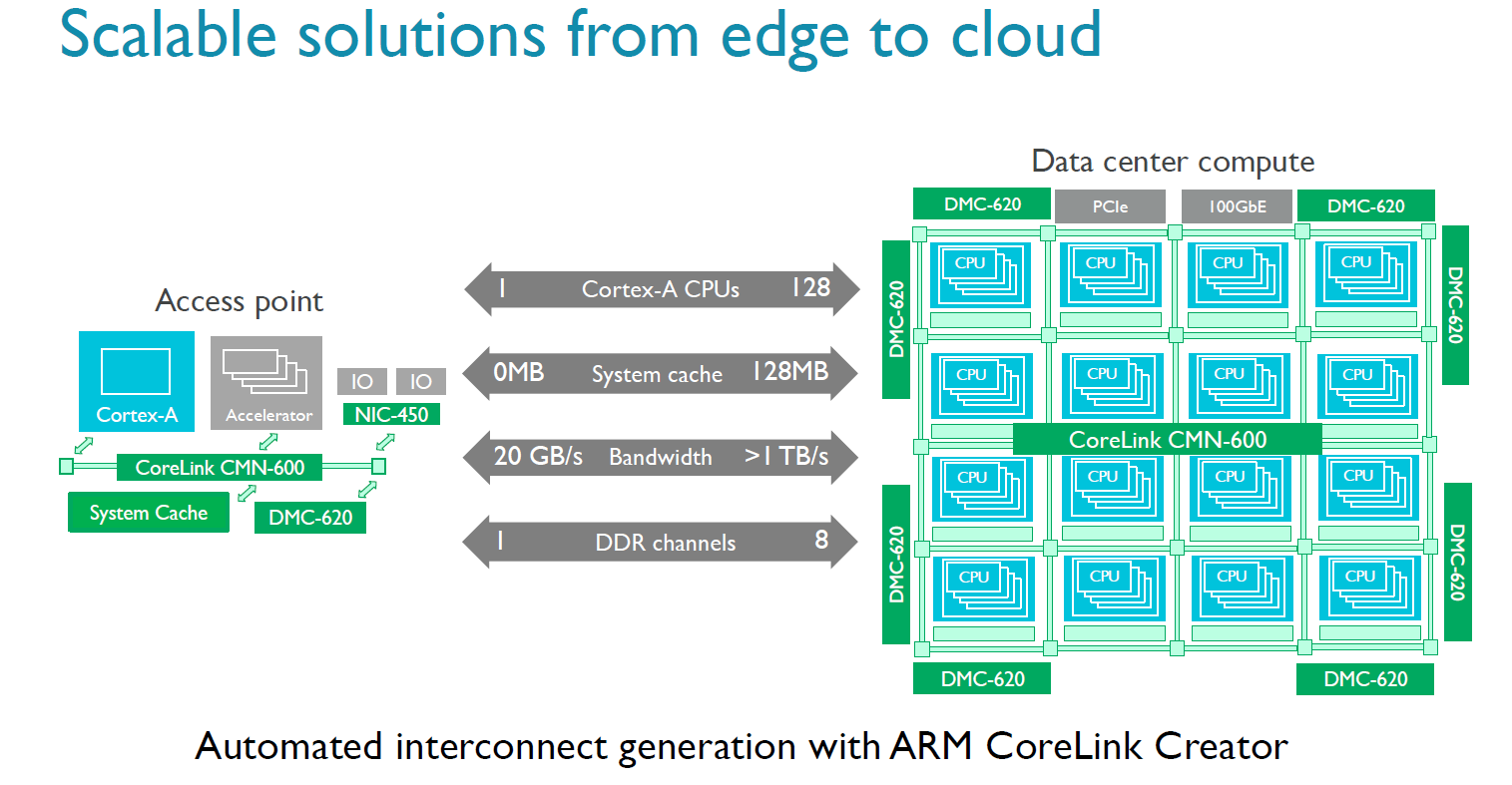
Also in the announcement is a new memory controller. The old DMC-520, which was limited to four channels of DDR3, is being superseded by the DMC-620 controller which supports eight channels of DDR4. Each DMC-620 channel can contain up to 1 TB DDR4, giving a potential SoC support of 8TB.
According to ARM through simulations, the improved memory controller offers 50% lower latency and up to 5 times more bandwidth. Also, the new DMC is being advertised as supporting DDR4-3200. 3200 MT/s offers twice as much bandwidth than 1600 MT/s, and doubling the channels offers twice the amount of bandwidth - so we can explain 4 times more bandwidth, so it is interesting that ARM claims 5x more, which would suggest efficiency improvements as well.
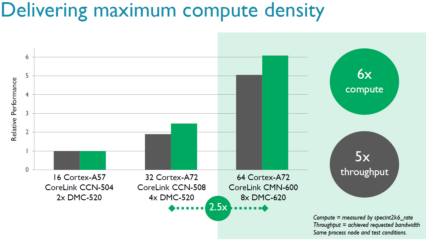
If you double the number of cores and memory controllers, you expect twice as much performance in the almost perfectly scaling SPEC int2006_rate. ARM claims that their simulations show that 64 A72s will run 2.5 times faster than 32 A72 cores, courtesy of the improved memory controller. If true, that is quite impressive. By comparison, we did not see such a jump in performance in the Xeon world when DDR3 was replaced by DDR4. Even more impressive is the claim that the maximum compute performance of a 64x A72 SoC can go up by a factor six compared to 16x A57 variant. But we must note that the A57 was not exactly a success in the server world: so far only AMD has cooked up a server SoC with it and it was slower and more power hungry than the much older Atom C2000.
We have little doubt we will find the new CMN-600 and/or DMC-620 in many server solutions. The big question will be one of application: who will use this interconnect technology in their server SoCs? As most licensees do not disclose this information, it is hard to find out. As far as we know, Cavium uses its own interconnect technology, which would suggest Qualcomm or Avago/Broadcom are the most likely candidates.
Source: ARM


14 Comments
View All Comments
shelbystripes - Tuesday, September 27, 2016 - link
So this enables putting 128 ARM cores on a single piece of silicon? Even with little cores and 14nm process, that's going to be a pretty large die.This would be pretty cool for building a BIG.little supercomputer though. A small block of 4 big cores to manage the OS and task scheduling, and then 124 little cores in parallel... Add a high speed interconnect to talk to other nodes and external storage servers, and you've got an entire HPC node as an SoC. Want a half million ARM cores in a single 19" rack?
Arnulf - Tuesday, September 27, 2016 - link
A quad A72 is 8 mm^2 in size (this includes L2 cache) on TSMC 16FF+.128 A72 cores would come out to 256 mm^2, not accounting for the interconnects and the rest of the chip. TSMC is manufacturing bigger GPU chips on this process so this is not unfeasible at all ...
ddriver - Tuesday, September 27, 2016 - link
Half the die of consumer chips is graphics, remove graphics and suddenly you have plenty of room for cores.jjj - Tuesday, September 27, 2016 - link
A73 on 10nm is under 0.65mm2, a quad cluster with 2MB L2 some 5mm2,add a large L3 and it's still small.But the real push in server is for 7nm HPC and bigger cores.
name99 - Tuesday, September 27, 2016 - link
Yeah, people are totally confused about how large (or rather small) CPU cores are.Even the A10 core, eyeballing it from the die shot, is perhaps 14 to 16mm^2 (including 2 fast cores, 3MiB L2, and two companion cores; L3 adds maybe 30% more).
Not as small as A72s, but again it would be totally feasible to put 16, maybe even 24, of these (2+2) units, and L3, on a die if you had the urge to do so. The details would start to depend on howmuch else you also want to add --- memory controllers, what IO, etc.
The high end of die size is up at 650mm^2 or so, as opposed to 100 to 150mm^2 at the low-mid end (eg the range of Apple's mobile and iPad SoCs).
Obviously you pay serious money for that sort of large size, but it is technically quite feasible and is used.
patrickjp93 - Thursday, October 6, 2016 - link
Cache is the expensive part, and you're going to need an L3 cache to keep such a cluster fed, whether it's a victim cache or a primary.TeXWiller - Tuesday, September 27, 2016 - link
ARM press release talks only about the interconnect bandwidth increase of five times, not about a similar increase in memory bandwidth. They do support 3D stacked ram though (HBM, HMC?), so that might explain the number.T1beriu - Wednesday, September 28, 2016 - link
Have you even read anything from this announcement?!TeXWiller - Wednesday, September 28, 2016 - link
Is there a source for those simulated memory controller results somewhere, a release event or an interview? News release talks about throughput related to interconnect bandwidth on the whole, not specifically that related to the memory controller like this article suggests.jjj - Tuesday, September 27, 2016 - link
Don't forget that on the slide the A57 is on the same process so real world A57 on 28nm is not the baseline.