Testing Samsung 850 Pro Endurance & Measuring V-NAND Die Size
by Kristian Vättö on July 7, 2014 1:20 PM ESTV-NAND Die Size: Bigger Than What We Initially Thought
In our 850 Pro review, I did some calculations to estimate the die size of the second generation V-NAND based on the first generation V-NAND. As some of our clever readers pointed out, the die size does not scale perfectly with the die capacity because the peripheral circuitry cannot be scaled as aggressively as the capacity can be. As a result, my initial estimation ended up being way too small because I did not take the scaling of the peripheral circuitry into account.
Unfortunately, Samsung would not disclose the die size during the Q&A at the SSD Global Summit so I had to seek for an alternative way to figure out the correct die size. In the showroom, Samsung had the second generation 32-layer V-NAND wafer, which actually gives us everything we need to calculate a fairly accurate estimation of the die size.
The picture on top shows what the wafer looks like. It does not look any different from the typical 2D NAND wafer, which should not be a surprise given that the change happened deep inside. And no, the V-NAND wafer is not thicker than any normal wafer (at least not by eye) because the V-NAND stack is still in the order of microns.
As for the die size, I calculated 44 dies in the vertical direction, which means that with a 300mm wafer the depth of a single die is approximately 6.8mm.
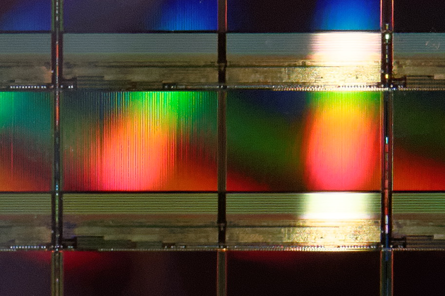
Courtesy of PC Perspective
To figure out the width of the die, you can either count the dies in the horizontal direction or go with the lazy route and just calculate the proportion of the depth and width. Allyn Malventano from PC Perspective was able to grab this awesome photo of the die itself, so I used the ruler tool in Photoshop to measure the size of the die along both X and Y axes and it appears that the width of the die is about 2.05 times its depth (note that it is a two-plane design). In other words, the die size is around 6.8mm x 14.0mm, which works out to be 95.4mm2.
| NAND Die Comparison | ||||
| Samsung 1st Gen V-NAND | Samsung 2nd Gen V-NAND | Micron 16nm NAND | Toshiba A19nm NAND | |
| Die Capacity | 128Gbit | 86Gbit | 128Gbit | 64Gbit |
| Die Size | 133mm2 | ~95.4mm2 | 173mm2 | 94mm2 |
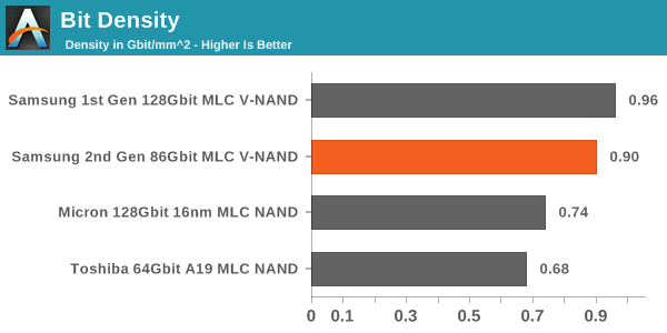
Here is an updated bit density graph. Even with the updated, larger die size, V-NAND is noticeably denser than 2D NAND, although the first generation appears to be more dense. I am guessing the smaller die size is better for yields (larger chips have higher probability of manufacturing errors), which makes the second generation more cost efficient despite the slightly lower density.


39 Comments
View All Comments
isa - Monday, July 7, 2014 - link
A thoughtful article, Kristian. As an ex-ASIC designer, I agree with your assessment that the SMART value is likely being manipulated by Samsung - no competent IC fab would have the bimodal yield variability that would otherwise account for the 2x SMART value versus the 10x marketing claim. If the result was in fact based on yield variability, then you'd see a range of SMART decimation values for a range of samples. But if all the drives report a consistent 2x effect, then it's being manipulated.emvonline - Monday, July 7, 2014 - link
Great article and comments Kristian! just what I was looking for.... Thanks!The lateral spacing is far larger than expected with 40nm lithography and hence the cell density is much lower than expected for theoretical VNAND.
Most companies think 3D NAND makes sense only with 256Gbit to be cost effective. Lower densities get expensive due to array efficiency. IMO, Samsung is introducing a new part at high cost and high price so they can fix efficiencies later. smart move
FunBunny2 - Monday, July 7, 2014 - link
With regard to the 2X and 10X issue. Is Samsung claiming both numbers, in different places, specifically to NAND performance? Or is "endurance" an SSD number, which would encompass controller logic, spare area, and such, thus 10X while raw NAND performance is 2X?mkozakewich - Tuesday, July 8, 2014 - link
In the world of enterprise and the government, you don't generally want things failing unexpectedly. Most tolerance standards incorporate that truth, so you get ratings that aren't even close to failure at their maximums.I assume that's what's going on here. It seems weird that AnandTech is acting incredulous about it, because they specifically called it out when testing other (Intel, I think?) drives. Basically, the wear-levelling factor usually means nothing. Like an expiry date on milk, you can be statistically assured that nearly all the products will be fine within that boundary. That the number is so low on these SSDs makes me think there's a large amount of variance in their samples, and it has to be that low to catch a high enough percentage to fit their failure tolerance.
That and I *think* they got the 10x number from a single drive Samsung was boasting about.
Sivar - Wednesday, July 9, 2014 - link
Units missing. Please add.1.10 what per day? 0.43 what?
Kristian Vättö - Thursday, July 10, 2014 - link
Drive writes per day, it's mentioned in the left-hand side column.LordConrad - Wednesday, July 9, 2014 - link
"... (GB in Windows is really GiB, i.e. 1024^3 bytes)..."Windows is correct to use GB. When a prefix (Giga) is used in front of a binary measurement (Byte), the resulting measurement remains binary. Hard drive manufacturers use of the prefixes is wrong (and done for the sole purpose of inflating their numbers), Windows is right, and GiB is a redundant measurement.
Zan Lynx - Wednesday, July 16, 2014 - link
You are right in your own imagination.SI units are SI units, period, end, stop.
sonicmerlin - Thursday, July 10, 2014 - link
Does this mean Samsung could deploy V-NAND on a 1X nm process and effect a 32x increase in density? Or even 2X nm process and 16x density increase? That would put them ahead of HDDs in terms of cost per bit, wouldn't it? Is there any reason they're not going down this path in at least the consumer market, where SSD endurance isn't a top priority?garadante - Friday, July 11, 2014 - link
Probably because they have no reason to absolutely crash the price/GB standard for SSDs. They'd have absolutely no competitors at that density in the immediate future so nobody could compete. And considering their current model allows them to just barely eke out densities ahead of competitors in order to give them the most competitive product (if barely) it allows them to continue to make profit on many generations of product rather than completely changing the entire industry in one sweep. Just like what Intel does with CPUs. Why give the consumer all the cards in your hand when you can tease them with a bare fraction of your true potential to get sales from them year after year over the next several decades?