Intel Details PowerVia Chipmaking Tech: Backside Power Performing Well, On Schedule For 2024
by Ryan Smith on June 5, 2023 9:00 AM EST- Posted in
- CPUs
- Intel
- EUV
- IFS
- Intel 20A
- Intel 18A
- PowerVIA
- Arrow Lake
- Backside Power
- Crestmont
At next week’s annual VLSI Symposium, Intel will be presenting a pair of highly-anticipated papers about their progress with their upcoming PowerVia chip fabrication technology – the company’s in-development implementation of backside power delivery networks. Along with Intel’s RibbonFET technology for gate-all-around transistors, PowerVia and RibbonFET are slated to serve as Intel’s big one-two punch to the rest of the silicon lithography industry, introducing two major chip technologies together that Intel believes will vault them back into the fab leadership position. Combined, the two technologies are going to be the backbone of Intel’s “angstrom” era fab nodes, which will go into high volume manufacturing next year, making Intel’s progress with the new technologies a subject of great importance both inside and outside of the company – and one which Intel wants to address.
When it comes to Intel’s chip manufacturing technology, the stakes for Intel’s R&D groups couldn’t be any higher than they are right now. The long-time leader of the fab would has faulted – repeatedly – and is now in the middle of a multi-year effort to course-correct, not only to get back that leadership position which they’ve lost, but to break into the contract chip manufacturing business in a big way.
As a result, while VLSI research papers do not normally attract a ton of outside attention, this year in particular is a big exception. With RibbonFET and PowerVia set to go into production next year, Intel is reaching the point where they’re wrapping up R&D work on the first generation of those technologies. Intel is now at the point where, to their peers in the VLSI industry, they can present their first findings around producing a complex logic test chip. And to Intel’s investors and other outsiders, Intel can show the first real evidence that their efforts to get back on track may very well be succeeding, giving Intel an opening to leap ahead of the competition that the company greatly needs.
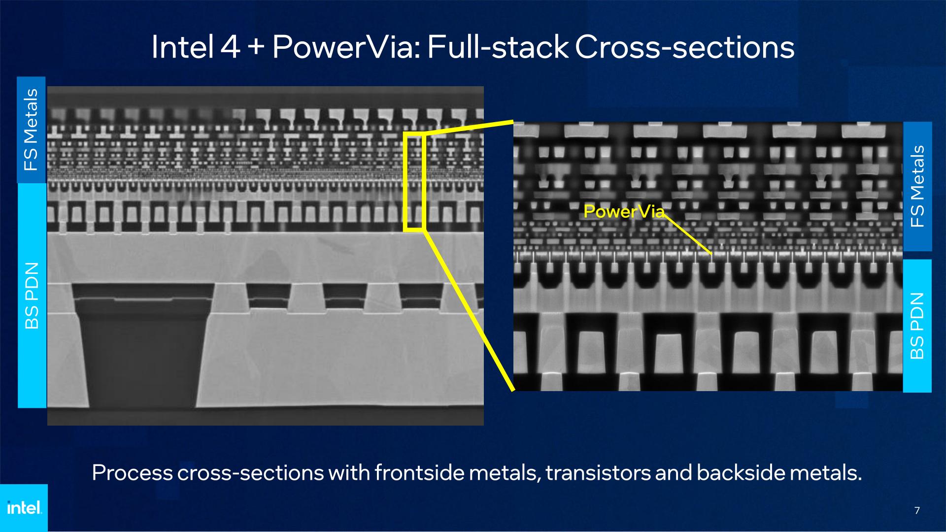
To that end, at next week’s symposium Intel is going to be disclosing a great deal of information around their implementation of backside power delivery network technology, which they call PowerVia. Central to these papers is Blue Sky Creek, an Intel “product-like” logic test chip that implements backside power delivery on the EUV-enabled Intel 4 process technology. With Blue Sky Creek, Intel intends to demonstrate that not only do they have PowerVia working with a CPU on time for high volume manufacturing next year, but that the performance and manufacturing benefits of backside power delivery are everything Intel has promised. Suffice it to say, Intel is preparing for this year’s VLSI conference to be a very big moment for the company.
Backgrounder: Backside Power Delivery
Backside power delivery networks (BSP/BS-PDN) is a technology concept that has been quietly in development for the past several years across the entire chip fab industry. Similar to EUV in recent fab nodes, BS-PDN is seen as an essential technology to continue developing ever-finer process node technologies, and as a result, it’s expected that all leading-edge chip fabs will move to the technology in the future.
With that said, they are not all moving there at the same time. Intel expects to be first of the big three chip fabs to productize the technology, bringing it into chips at least two years ahead of its competitors. As a result, Intel is very much the pathfinder for the technology, which comes with no shortage of risks – but it also comes with significant rewards for getting the technology (and their timing) correct. For Intel, the company believes that this will be their new FinFET moment – a reference to Intel’s introduction of FinFETs on 22nm in 2012, which cemented Intel’s lead in the market for several years. This is particularly important as Intel won’t have a lead over its competitors when it comes to gate-all-around FETs (GAAFET) timing, so BS-PDN/PowerVia is going to be Intel’s trump card in the fab space for the next few years.
Meanwhile, to fully understand how BS-PDN works, the best place to start is to recap how traditional (frontside) power delivery works, so that we can contrast that to the many changes that come with building a BS-PDN wafer.
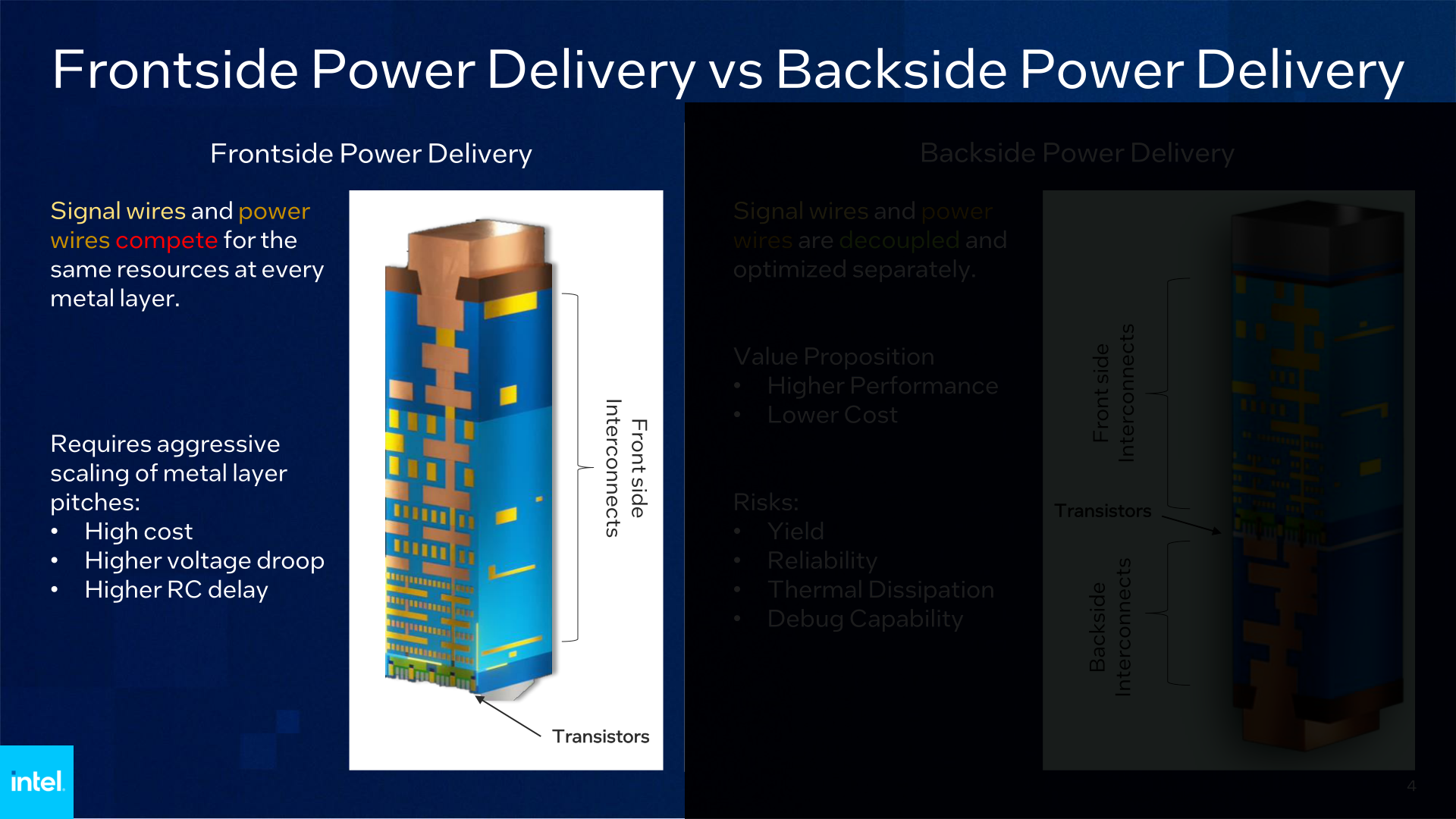
The manufacturing process of a modern, frontside power delivery chip starts with etching the transistor layer, M0. This is the smallest and most intricate layer on a die, and is where high-precision tools like EUV and multi-patterning are needed the most. In short, it’s the most expensive and complex layer of the chip, which has significant ramifications for both how chips are constructed and how they are tested.
Above that, additional metal layers are added at increasing sizes to account for all the wiring needed between the transistors and different parts of the processor (cache, buffers, accelerators), as well as providing routing for power that comes in from even further up the stack. Intel likens this akin to building a pizza, which is a crude analogy, but effective.
A modern high-performance processor typically has anywhere from 10 to 20 metal layers in its design. With the Intel 4 process in particular, there are 16 layers for logic, ranging from a pitch of 30 nm up to 280 nm. And then there’s another two “giant metal” layers on top of that just for power routing and placing external connectors.
Once a die has been fully fabbed and polished, the die is then flipped over (making this a flip chip) so that the chip can talk to the outside world. This flip places all the connectors (power and data) at the now-bottom of the chip, while the transistors end up at the top of the chip. Once flip chip manufacturing was mastered, this made chip debugging and cooling especially convenient, as it allowed debugging tools easy access to the all-important transistor layer. Meanwhile those hot little gates also became especially close to the chip’s cooler, allowing for the relatively easy transfer of heat out and away from a chip.
The drawback with frontside power delivery, however, is that it means both power and signal wires are on the same side of the chip. Both wires have to take a significant trip down through 15+ layers to reach the transistors, all the while competing for valuable space and creating interference with each other. For the power wires in particular, this is especially a nuisance, as the resistance along these wires causes the voltage of the incoming power to drop, which is known as the IR Drop/Droop effect.
For most of the history of chip fabbing, this hasn’t been a huge issue. But like so many other aspects of chip building, the problem has become more and more pronounced as chip feature sizes have shrunk. There is no obvious hard limit here on frontside power delivery, but given how much harder it is to shrink chips with every successive generation, the problem has become too big (or rather, too expensive) to work around.
And that brings us to backside power delivery. If having both signals and power coming in on the same side of the chip is causing problems, why not separate the two? This, in a nutshell, is exactly what backside power delivery looks to resolve, by moving all of the power connections to the other side of the wafer.
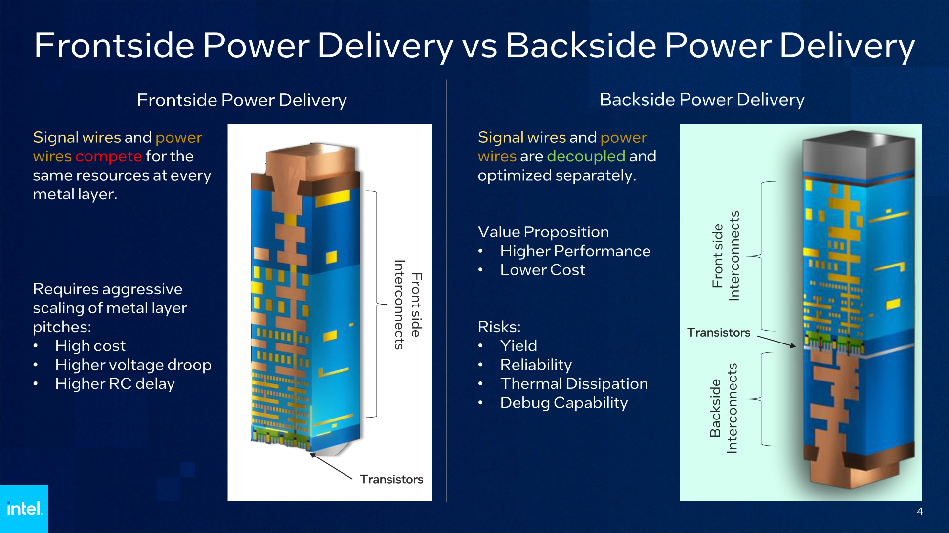
For Intel’s PowerVia implementation of this concept, Intel quite literally flips a wafer upside down, and polishes away almost all of the remaining silicon until they reach the bottom of the transistor layer. At that point, Intel then builds the metal layers for power delivery on the opposite side of the chip, similar to how they would have previously built them on the front side of the chip. The net result is that Intel ends up with what’s essentially a double-sided chip, with power delivery on one side and signaling on the other.
On paper (and in Intel’s paper), there are ultimately several benefits to moving to BS-PDN. First and foremost, this has a meaningful impact on simplifying the construction of a chip. We’ll get to Intel’s specific claims and findings in a bit, but of particular note here is that it allowed Intel to relax the density of their M0 metal layer. Rather than requiring a 30 nm pitch on Intel 4, Intel’s test node for Intel 4 + PowerVia allowed for a 36 nm pitch. That directly simplifies the most complex and expensive processing step of the entire chip, rolling it back to something closer in size to the Intel 7 process.
BS-PDN is also primed to deliver some modest performance improvements to chips as well. Shortening the route for power delivery to the transistors with something more direct helps to counteract the IR Droop effect, resulting in better power delivery to the transistor layer. And getting all of those power delivery wires out of the signal layers improves the performance of those as well, eliminating the power interference and giving chip designers more room to optimize their designs.
Otherwise, the trade-off for all of this is primarily in losing the previously mentioned perks of building a frontside chip. The transistor layer is now roughly in the middle of the chip, rather than at the end. This means that traditional debugging tools can’t directly poke the transistor layer of a completed chip to test it, and there is now 15 or so layers of signal wires between the transistor layer and the cooling service. These aren’t insurmountable challenges, as Intel’s paper takes care to lay out, but were issues that Intel had to work around in their design.
Manufacturability is the other set of trade-offs involved in moving to BS-PDN. Building power layers on the backside of a die is something that’s never been done before, which increases the chance of something going wrong. So not only does power delivery need to work, but it needs to work without significantly reducing chip yields or otherwise making chips less reliable. But if all of these things pan out, then the extra effort of building power layers on the backside of a wafer are more than cancelled out by the time and cost savings of not having to route power in through the front side.
Intel’s Added Wrinkles: Carrier Wafers & Nano TSVs
Because backside power delivery networks are going to become an industry standard feature in due time, we’ve tried not to focus too much on Intel’s specific implementation of BS-PDN/PowerVia. But now that we’ve hit the fundamentals of BS-PDN, there are a couple of Intel-specific implementation details worth noting.
First and foremost, Intel is using a carrier wafer as part of their construction process in order to provide chip rigidity. Bonded to the front side of a PowerVia wafer after the fabrication of that side is completed, the carrier wafer is a dummy wafer to help support the chip while Intel is blasting away at the other side. Because the two-sided chipmaking process polishes away so much of the remaining silicon wafer, there isn’t much structural silicon to hold the whole thing together. As Intel lightly jokes, despite this being silicon lithography, there’s only a tiny amount of silicon left on the wafer by the end.
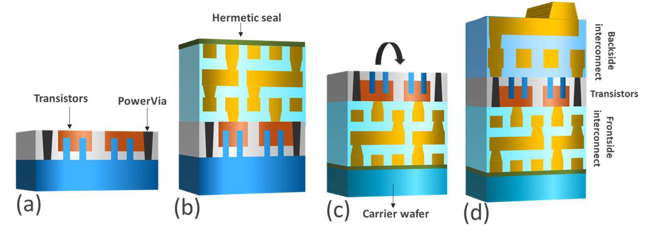
That carrier wafer, in turn, remains as part of the chip for the rest of its life. Once chip fabbing is completed, Intel can polish the bonded carrier wafer down to the necessary thickness. Of note, because the carrier wafer is on the signal side of the chip, this means it presents another layer of material between the transistors and the cooler. Intel’s techniques to improve heat transfer take this into account, but for PC enthusiasts accustomed to transistors at the top of their chip, this is going to be a significant change.
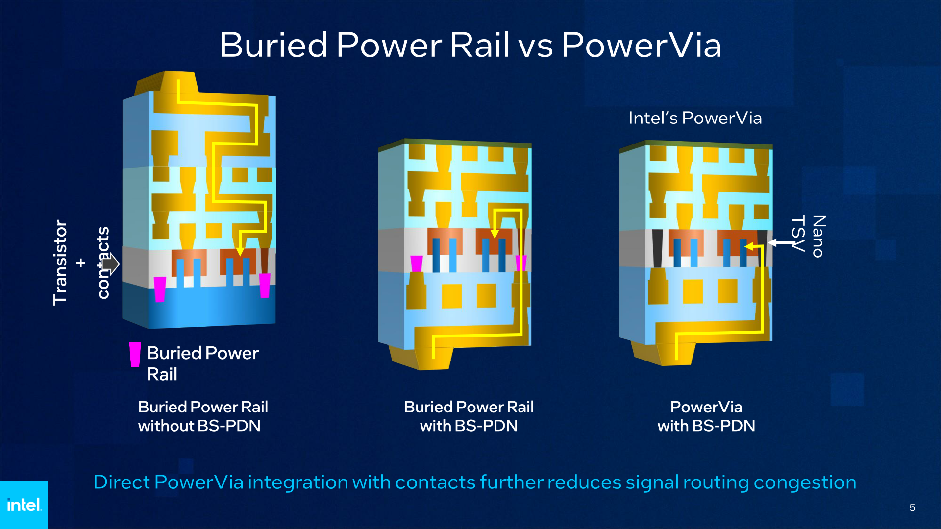
Intel’s other notable detail with their implementation of BS-PDNs is the use of TSVs for power routing. In PowerVia, there are nano-scale TSVs (aptly named Nano TSVs) in the transistor layer of the chip. This is in contrast to buried power rails, which is what industry pioneer IMEC has been looking into with their BS-PDNs.
The long and short of matters is that while power rails still required going up-and-over the transistor layer to deliver power, the use of TSVs allows power to be delivered more directly to the transistor layer. For Intel this is a technological advantage that they’re keen to exploit, as it avoids having to design and build-in the routing required for buried power rails.


31 Comments
View All Comments
obed51815 - Thursday, July 20, 2023 - link
Thanks for sharing this post! It's fascinating to see Intel's ambitious plans with PowerVia chip fabrication technology and RibbonFET for gate-all-around transistors. Considering the importance of these technologies in regaining their fab leadership position, Intel's R&D efforts must be at an all-time high. With the stakes so high, their progress in these areas becomes crucial not only for the company but for the entire industry.The upcoming VLSI Symposium is undoubtedly going to be a significant event, drawing attention both inside and outside the company. As Intel moves closer to the production phase, presenting their findings on producing a complex logic test chip becomes a crucial milestone. This evidence of progress will be reassuring to investors and other outsiders, showing that Intel's efforts to get back on track are bearing fruit.
It's impressive to witness the culmination of years of hard work and research, which will eventually bring the "angstrom" era fab nodes into high volume manufacturing next year. Embracing these new technologies could propel Intel forward and potentially position them ahead of the competition, as they venture into the contract chip manufacturing business.
In conclusion, Intel's advancements in chip manufacturing technology are vital for the future of the company and the industry as a whole. We eagerly await the outcomes of the upcoming symposium and wish Intel the best in their journey towards technological excellence.