Qualcomm Details The Snapdragon 888: 3rd Gen 5G & Cortex-X1 on 5nm
by Andrei Frumusanu on December 2, 2020 10:00 AM EST- Posted in
- Mobile
- Qualcomm
- Smartphones
- SoCs
- 5G
- Cortex A78
- Cortex X1
- Snapdragon 888
Hexagon 780: A Whole new IP for AI & DSP
Every year Qualcomm likes to talk about its new Hexagon DSPs, with the last few generations also adding to the table new Tensor Accelerators dedicated for ML inferencing. This year’s Snapdragon 888 design also hypes up the new Hexagon 780 design, with the difference being that this time around the generational improvements are truly humongous.

The new Hexagon 780 accelerator IP truly deserves a large increment in its IP numbering scheme, as it’s essentially a ground-up redesign of the company’s existing DSP with scalar and vector execution engines, and the recent Tensor Accelerators. Previously all these execution engines were acting as discrete independent blocks within the Hexagon 600 series family, but that’s now changed in the new IP design.
The new IP block fuses together all the scalar, tensor, and vector capabilities into a single monolithic IP, vastly increasing the performance and power efficiency of workloads that make a use of all the mixed capabilities of the design.
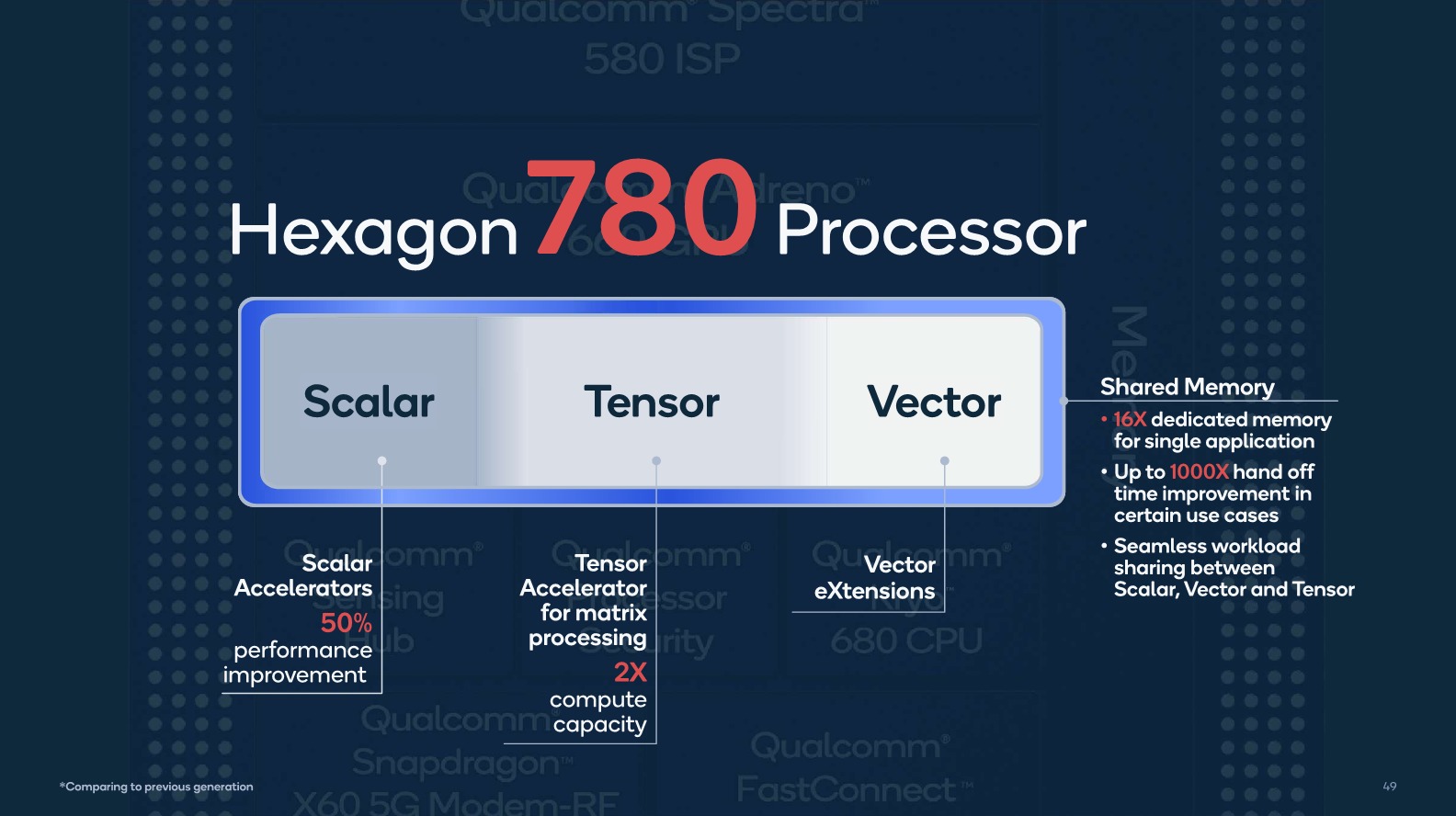
In terms of performance uplifts, scalar execution capabilities are said to be increased by 50%, while tensor execution throughput has doubled. The vector extension units seem to have remained the same this generation, but actual performance of workloads will still have been increased thanks to the new memory architecture of the new IP block.
Qualcomm states that they’ve increased the on-chip SRAM dedicated to the block 16-fold, allowing for larger machine-learning inference models to fit within the block’s memory, greatly accelerating their performance. This larger memory pool also allows for coherency between the scalar, vector and tensor units, allowing for the vastly increased workload handoff time between the different execution engines. I asked about the actual size of this new memory, but the company wouldn’t disclose any further details, just stating that it’s significant.
The company’s engineers were extremely hyped up about the new design, stating that the performance and flexibility of the new design is well beyond that of what other companies can achieve through disaggregated DSP and ML inference engines, sometimes even from different IP vendors.
The most important figure for the new design is the 3x performance per watt claim, which is just a massive generational improvement that you rarely see in the industry.

As is usual for Qualcomm, the company doesn’t actually state the per-block performance increases, but instead opts to showcase an aggregate computational throughput figure shared amongst all of the SoC’s IP blocks, including CPU, GPU, and the new Hexagon accelerator block. This new figure lands in at 26TOPs for the Snapdragon 888, which is 73% higher than the 15TOPs figure of the Snapdragon 865. Given that we’ve seen significant changes in all IP blocks this generation, I won’t attempt a breakdown estimate as it’s likely going to be wrong and off-the-mark anyhow.
The Adreno 660 - A 35% faster GPU
Amongst the improvements which lead up to that 26TOPs figure is a new vastly improved GPU in the form of the new Adreno 660.
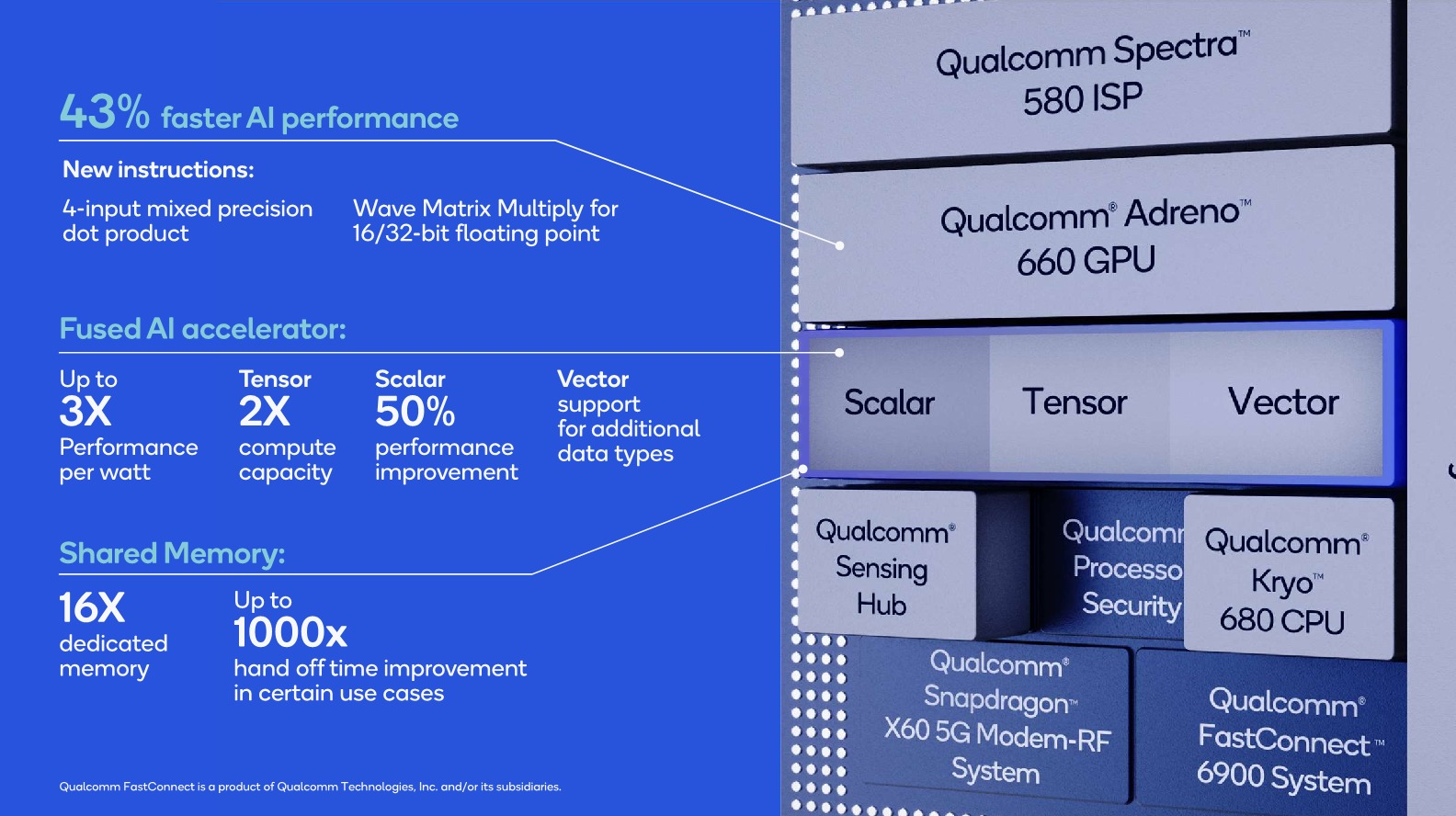
Qualcomm still holds architectural details of their GPUs very close to their chest and thus doesn’t go disclose very much about the new GPU design and what has actually changed, but one thing they did talk about is the addition of new mixed-precision dot product as well as FP16/FP32 wave matrix-multiply instructions, which allow the new GPU to increase AI performance by up to 43%.
We’re also seeing the addition of variable rate shading (VRS) onto the Adreno GPU architecture, allowing for coarser pixel shading onto larger pixel blocks for object and screen areas which don’t require as much detail or the native resolution shading wouldn’t be noticeable. This is also a major feature that’s being introduced in the console and new-generation PC graphics cards and GPUs, which should bring greater performance uplift for new gaming titles which take advantage of the new features. It’s great to see Qualcomm bringing this to the mobile space along with the rest of the industry.
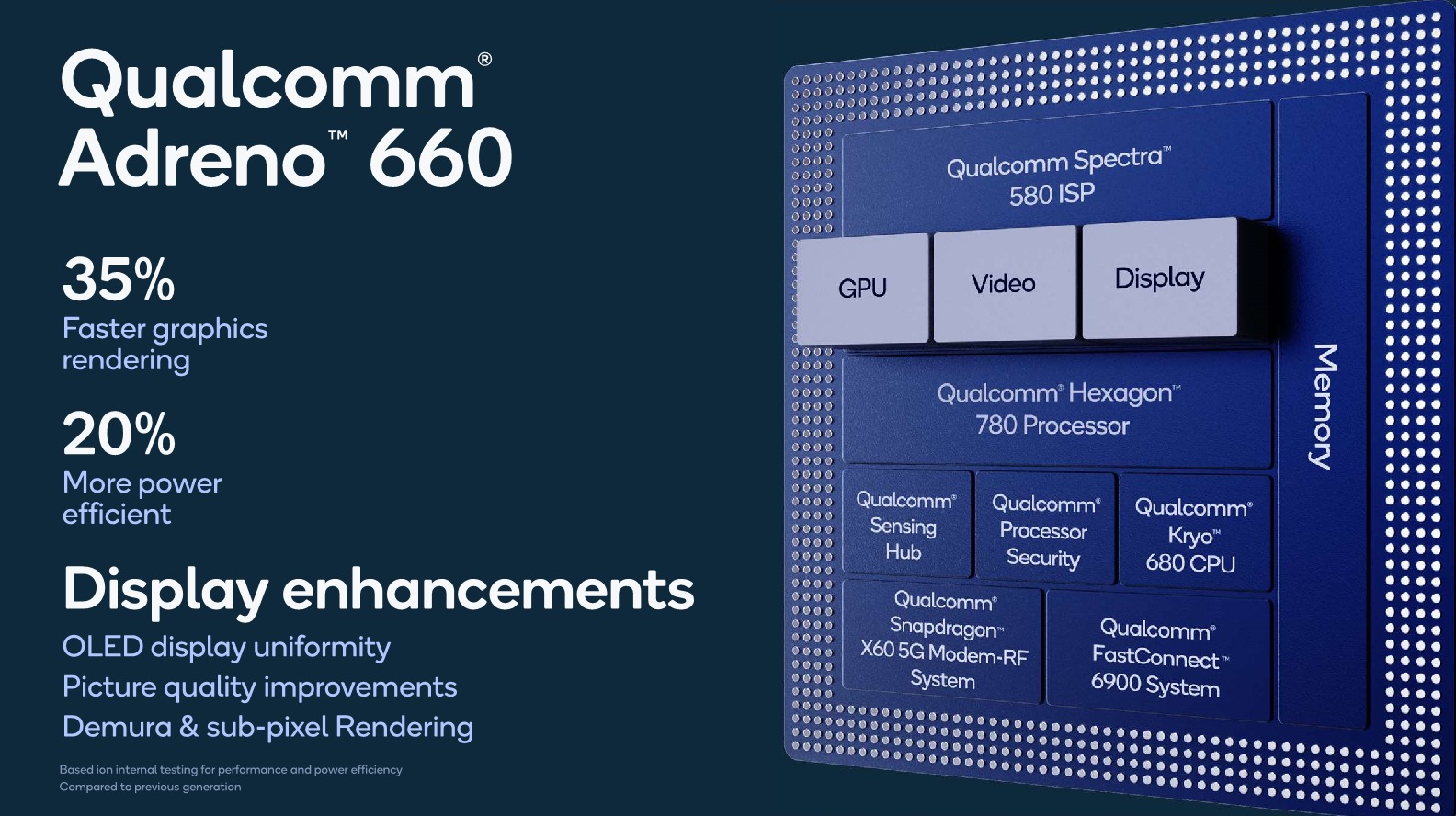
For graphics workloads, the new GPU is advertised as being able to increase performance by up to 35%, which is a very major generational performance leap.
Such a performance jump would actually signify that Qualcomm may very well regain the gaming performance crown this generation, having lost it to Apple’s SoCs over the last two generations. Apple’s latest A14 has seen rather conservative gains on the GPU side this year, so a 35% performance gain over the Snapdragon 865 should very much allow the new Snapdragon 888 to retake the leadership position.
A 35% performance increase with a 20% power efficiency increase would indicate that the new SoC would achieve the higher performance at cost of a little higher power consumption, but given the Snapdragon 865’s excellent power characteristics of below 4W, Qualcomm does have a little leeway to increase power this generation.
3200MHz LPDDR5
The new Snapdragon 888 moves from a hybrid memory controller to one that focuses on LPDDR5, and also increases the frequency support for new LPDDR5 to 3200MHz (Or LPDDR5-6400).
For the Snapdragon 865 Qualcomm was rather unenthusiastic about the LPDDR5 switch, saying that it didn’t bring all to great improvements to performance or power efficiency – something which we actually did test out and come to the same conclusion in our review of the two OnePlus 8 phones, where the LPDDR4X variant ended up being no slower and seemingly actually more efficient to us. Apple this year also kept on using LPDDR4X on their A14 and M1 SoCs – pointing out that the benefits aren’t all that great.
For the Snadpragon 888 however, Qualcomm’s engineers seemed more upbeat about LPDDR5 and the new SoC actually being able to utilise the increase memory bandwidth this generation. Without going into details, the company also stated that they’ve improved the overall design of the memory subsystem, improving aspects such as latency.
On the part of the memory subsystem, Qualcomm still employs a 3MB system-level-cache in front of the memory controllers, with the ability of all SoC IP blocks to take advantage of this cache.


123 Comments
View All Comments
lmcd - Wednesday, December 2, 2020 - link
820 was absolutely a disaster. Its errata list was too great for Windows kernel support, likely at the ISA implementation, and likely deeply-rooted enough to justify dropping the entire endeavor.Silver5urfer - Wednesday, December 2, 2020 - link
How is Windows Kernel coming into the picture ?It was about the Android performance and 64Bit compat due to Apple's move first and 810's ultimate disaster which even killed HTC entirely. 820 processor was very fast and still holds up, just like 805 but the latter was 32bit, One can see comparison of that with Apple's A9.
Entire endeavor was dropped because there's no need. Why do you think Qcomm develops a lot of the Radio and etc and tons of R&D ? Patents. That's what Qcomm is all about and they tried that with Centriq. But ARM on DC market is a dead end, so many years of articles here on AT and STH, so far no one is there on that side the only option which was showing some metric of performance that too for small loads is Graviton2. Only when there's a need then these companies push, which is money. Apple does it because they want to hold that position to leverage their pricing justification of the iPhone. Looking at any Android top flagship vs iPhone real world application performance tests and gaming loads it shows why there is no need for Qcomm to push, they push where there is money, GPU and NPU, ISP, Radio RF.
techconc - Thursday, December 3, 2020 - link
Qualcomm and Samsung had different problems with their CPU designs. Qualcomm had a pretty competitive design. Their problem was getting blind-sided by the A7 with 64bit. They didn't have a 64bit design in their pipeline and had to abandon their own work and go back to ARM reference designs just to have something remotely competitive.Samsung found out the hard way that chip design isn't easy. Making a more powerful chip is one thing, but being energy efficient (and powerful) is quite another thing. They eventually scuttled their custom chip hopes as well.
That leaves ARM. ARM will design what their customers want. It's not clear that customers are complaining to ARM that they want more powerful cores. Maybe the X1 is a step in that direction. However, we can see lots of cost cutting examples in the SD888, so it's not clear that there is an appetite for an Apple like design for Android based SoC vendors.
ZolaIII - Thursday, December 3, 2020 - link
A55 is not inferior, it's still the best in order A core ARM ever made. The so called Apple little core's are simple OoO core's inferior but closest to compare to A73. Problem is ARM never made a newer incarnation of A73 suitable for DynamIQ clusters. They did make Neoverse E1 and A65 which both thanks to SMT aren't exactly suitable for mobile phones and we didn't see any of their actual silicone implementations.I don't see a L3 victim cache as the way to go as it's limiting in many aspects. Faster RAM & bigger L2 cache should be a way to go.
Apple just makes your wallet cry.
AntonErtl - Thursday, December 3, 2020 - link
The A75 is derived from the A73 (3-wide instead of 2-wide), and AFAIK supports DynamIQ. And looking at Andrei's M4 review, the A75 appears to be almost as efficient as the A55 at the A55's lowest voltage, and more efficient if the A55 has to ramp up the voltage (long before it reaches the performance of the A75 at its lowest voltage).Wilco1 - Friday, December 4, 2020 - link
Even better would be a low clocked and slightly cut-down Cortex-A76. According to AnandTech at lower frequencies it is more efficient than Cortex-A55 while being much faster. It has a larger area of course, but you could cut it down a bit, and 4 little cores seems a bit overkill, 1 or 2 would be more than enough for background tasks.Irish910 - Monday, December 14, 2020 - link
Apple efficiency cores have much better performance and power efficiency versus other chips with a similar design. (High perf/low perf).It’s amazing to see what Apple has achieved since the A9 year over year just dominating performance while keeping power efficiency. It’s not even close with Apple GPUs.
You’ll probably squabble that Metal is more optimized than OpenGL.
When it comes to chip designs, whether you like apple or not, they are the best.
patel21 - Wednesday, December 2, 2020 - link
Was Samsung going to use AMD GPU this year ? It they do, I can see them wearing the Android Performance Crown easily.darkich - Wednesday, December 2, 2020 - link
I don't understand why they just don't ditch the A55 cores and use two underclocked A78s instead.The A78 is the most power efficient CPU on the planet at under 2GHz!..yes I'm not forgetting the Icestorm from Apple.
1X1 + 3A78 +2A78 should be optimal according to me..what am I missing?!
lmcd - Wednesday, December 2, 2020 - link
Die size considerations.What you're really identifying here is that the paragraph at the end of page 1 is extremely damning. Qualcomm isn't good enough with intricate work on multiple voltage planes to deliver a the best possible SoC.