The AMD Ryzen Threadripper 3960X and 3970X Review: 24 and 32 Cores on 7nm
by Dr. Ian Cutress, Andrei Frumusanu & Gavin Bonshor on November 25, 2019 9:05 AM ESTZen 2 Platform for HEDT - Improvements over Last-Gen
Section by Andrei Frumusanu
The platform architecture of the new Threadripper 3000 series is fundamentally different, and a massive departure from what we’ve seen in the past on the first and second generation Threadripper products. Previously, AMD still made use of its monolithic die design used in Zen and Zen+ Ryzen, Threadripper and EPYC products. The approach was an economically smart one for AMD in regards to having to design only a single silicon die that would be used across the three product lines, however it had some fundamental technical disadvantages when it came to power efficiency as well as having to make some performance compromises.
The biggest disadvantage exhibited by the Threadripper 2000 series was the platform’s weakness in regards to its memory architecture, an issue that was particularly prevalent in the 32-core Threadripper 2990WX. As explained in our review of the TR2 products last year, the main problem with that SKU was that in order to achieve a 32-core product, AMD had to make use of 4 “Zeppelin” dies. Unlike the server-oriented SP3 socket however, Threadripper products come on the TR4 platform. While the two sockets are physically identical, they’re electrically incompatible with each other. In practice, the biggest difference between the two platforms is the fact that Threadripper products supports 4-channel memory setups, while the EPYC variants support the full 8-channel memory configuration possible.
The main conundrum for a product such as the 2990X which had to make use of 4 dies, each integrating 2 memory controller channels, is the decision on how you split up the memory controller setup between the dies and choose which 4 active controllers you’ll end up using. AMD’s approach here is that instead of using only one memory controller per die, the company chose to have two dies each with both memory controllers active, while the other two dies wouldn’t have any memory controllers enabled at all. The issue here is that the CPUs located on these dies would only have to access memory by hopping through the infinity fabric to the adjacent dies which did have memory controllers, and incur quite a large memory latency and bandwidth penalty. This penalty was large enough, that in situations where applications weren’t properly NUMA-aware and scaled across all core, the 2990WX ended up sometimes lagging behind the 16-core 2950X in performance.
Chiplet Architecture To The Rescue
Of course, AMD was aware of this drawback, but wasn’t planning to stay with this compromise forever. The new Ryzen 3000 series earlier this summer introduced the chiplet architecture for the first time ever, with some quite astounding success. The main differences here is that AMD is decoupling the actual CPU cores and cluster from the rest of the traditional SoC. The CPU chiplet contains nothing more than the CPU cores themselves, the CPU clusters L3 caches, and the I/O interface which communicates with the rest of the “traditional” system, which is now located on a separate silicon die.

AMD Ryzen 3000 Consumer IOD - Credit Fritzchens Fritz
For the Ryzen 3000 products, this I/O die is seemingly quite familiar in terms of design to what we saw in the first- and second-generation Zen architecture products. We find your various I/O IP blocks which take care of various connectivity such as USB, Ethernet, SATA, alongside the critical components such as the PCIe controllers and of course the memory controllers. In general, what’s found on the Ryzen 3000 IOD isn’t all too different in functionality than what we previously saw on the monolithic Zen dies from past years – of course, except for the CPUs themselves.
AMD EPYC2 / Threadripper 3000 sIOD - Credit Fritzchens Fritz
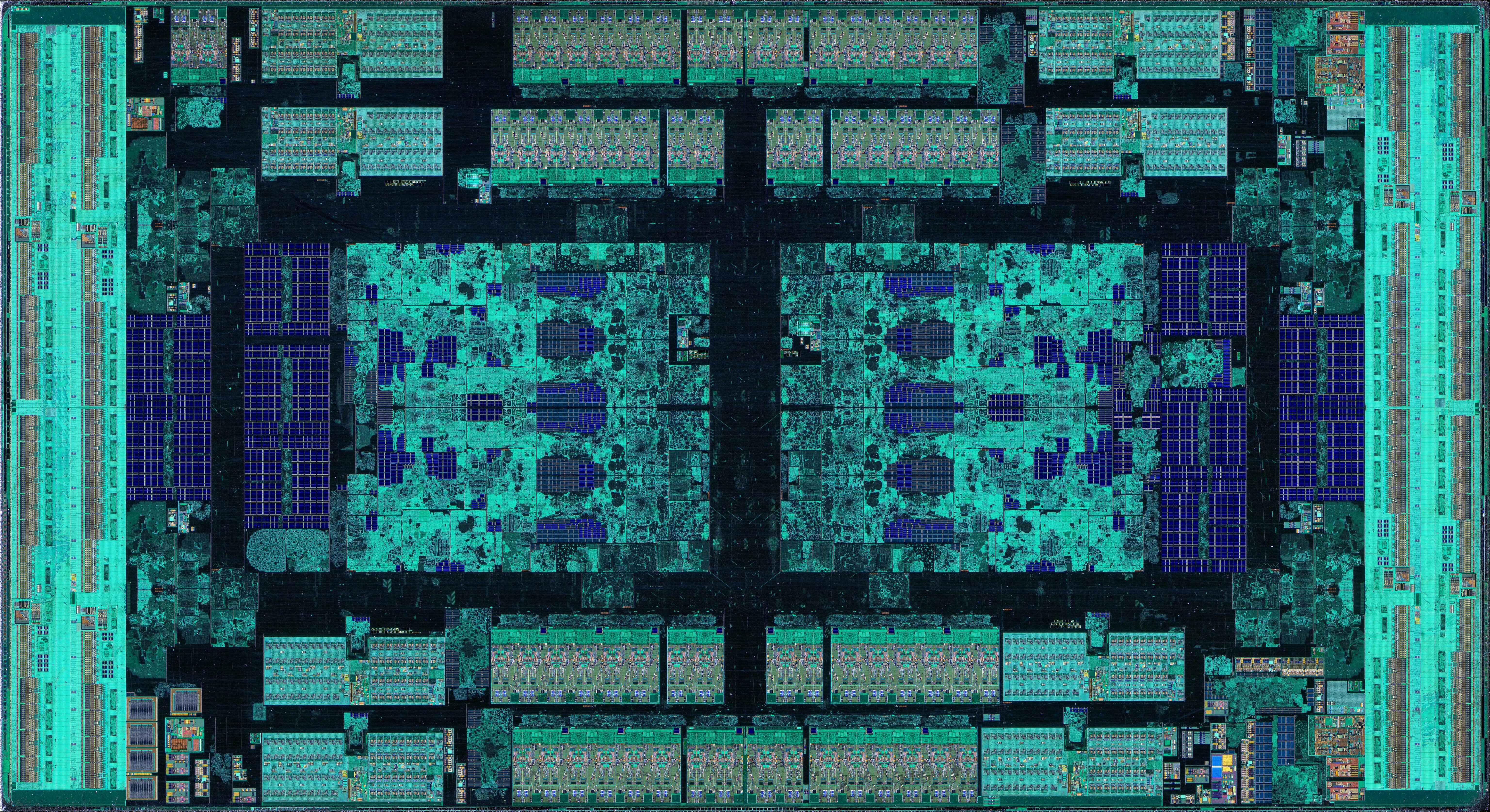
As we move on to the new Threadripper 3000 products (and new EPYC 2 processors), we however see the AMD’s main chiplet design advantage. Although the new Threadripper and EPYC products use the very same 7nm CPU chiplet dies (CCDs), they are using a different IO die, what seems to be called by AMD as the sIOD (server IO die?).
What’s interesting about the sIOD is that it’s not much of a “monolithic” design, but actually more similar to four consumer IO dies put together on one chip. In the above die shots (credit to Fritzchens Fritz), we actually see that AMD is employing an identical physical design of large parts of the chip’s IP blocks, with the main "central" block cluster going as far as being essentially identical. Of course, the layout of the various surrounding blocks is quite different. AMD here is essentially reusing design resources across its product ranges.
While the chip isn’t completely mirrored – there are still distinct unique IP blocks on each quarter of the die, it is in fact correct to say that it’s divided into quarters. These “quadrants” are in fact physically and logically separate from each other. Where this is important to consider, is in regards to the memory layout. In fact, logically, the layout is actually quite similar to what we’ve seen on the previous generation Threadripper and EPYC chips in terms of memory controller and CPU cluster distinction. Each quadrant still has its own two local memory controller channels, and the CPU CCXs connected to this quadrant have the best latency and bandwidth to memory. The CPUs accessing memory controllers of a different quadrant still have to do this via a hop over the infinity fabric, the biggest difference for this generation however is that instead of this hop being across different dies on the MCM package, it all remains on the same silicon die.
For Rome, AMD had explained that the latency differences between accessing memory on the local quadrant versus accessing remote memory controllers is ~+6-8ns and ~+8-10ns for adjacent quadrants (because of the rectangular die, the quadrants adjacent on the long side have larger latency than adjacent quadrants on the short side), and ~+20-25ns for the diagonally opposing quadrants. While for EPYC, AMD provides options to change the NUMA configuration of the system to optimize for either latency (quadrants are their own NUMA domain) or bandwidth (one big UMA domain), the Threadripper systems simply appear as one UMA domain, with the memory controllers of the quadrants being interleaved in the virtual memory space.
The interesting question here of course is, how is this UMA domain setup for the Threadripper 3950X and 3970X? The SKUs come with 4 chiplets each, with the 3950X employing 3 cores per CCX, totalling 24 cores, and the 3970X employing 4 cores per CCX, totaling 32 cores. However, what we don’t know is how these chiplets are divided and populated across the sIOD’s quadrants. In theory, one could have one chiplet and one memory controller per quadrant – or one could have just two fully populated quadrants with the other two quadrants disabled. Given we have numbers on a fully populated EPYC 7742 to compare against, and that the diagonally opposing quadrant latency penalty is quite big, we should be able to estimate the implementation based on the latency results.
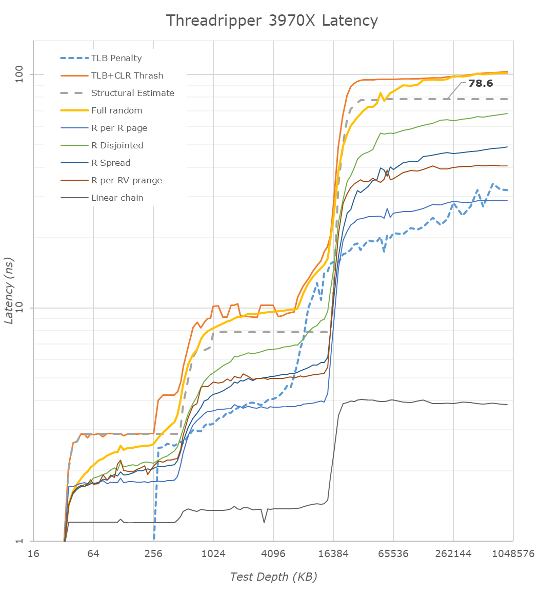
Looking at the latency results, there’s a few comparisons to make. In regards to the L1, L2 and L3 performance, I refer to our original Zen2 analysis in our Ryzen 3000 review article. The numbers here don’t change, which is natural as we’re talking about the very same CPU chiplet across the different product lines.
Going out of the CCD, the DRAM latency is the most interesting difference that we need to have a closer look at. Comparing the new Threadripper 3970X to the 2950X we see a latency degradation of 16.2ns, with the structural DRAM latency rising from 62.2ns to 78.6ns. For this comparison we’re using the very same DRAM sticks with identical timings between the Ryzen and two Threadripper platforms, so any differences here are solely due to the architectural differences of the platforms.
This degradation is actually to be expected. The third generation Threadripper degrades in two aspects compared to its predecessor: First of all, the chiplet architecture does incur a latency penalty as the separation of the CPU cores onto a different silicon die comes with a latency penalty. Secondly, in the first and second generation Threadripper products, each CPU had access to its own die memory controller by default, and it wasn’t possible to use an UMA setup. The third-gen Threadripper comes with an UMA setup by default, and the fact that the IOD is interleaving memory accesses across the quadrant memory controllers again adds another latency penalty.
Looking at the differences between the EPYC 7742 running in NPS4 mode and the new 3970X, we however see that the new TR3000 platform has a definitive latency advantage of almost 25ns – albeit we’re no longer running apples-to-apples here in regards to the DRAM.
Finally, the most interesting comparison is using the very same DRAM and timings between a Ryzen 3000 processor and the new 3970X. Using an 3700X we had at hand, the latency penalty for the new TR chip is “only” 9.2ns, rising from 69.4ns to 78.6ns. Maybe I might sound a bit optimistic here, based on the Rome numbers from earlier this summer I had expected some quite worse results for the new Threadripper 3000 series, so I see this result to be actually quite good. While we don’t have definitive confirmation, it does look like the new 24 and 32-core Threadripper 3000 SKUs are using only two adjacent quadrants of the sIOD.
Of course, the structural latency degradations here don’t necessarily translate to performance degradations. As we saw on the Ryzen 3000 products, AMD’s new doubled L3 cache as well as improved prefetchers have managed to more than compensate for the worse structural latency, actually increasing the memory performance of the new Zen2 chips.


245 Comments
View All Comments
schujj07 - Tuesday, November 26, 2019 - link
Where I work we now have 4x Dual 32 Core Epyc 7502s and 2x Dual 24 Core Epyc 7401s. We cannot move to Server 2016/2019 due to the per core licensing. However, for our VMware environment it is amazing how many VMs just 1 of those hosts can run.Supercell99 - Tuesday, November 26, 2019 - link
Is vmware stable on the new Epycs? I have some older Dells R630 2697 x2 I need to upgrade running ESXi 6.0 A bit nervous about jumping to AMD for production on vmware.schujj07 - Tuesday, November 26, 2019 - link
They are perfectly stable. We are running them for production work. 2nd Gen Epyc is only supported on 6.7 U3.Foeketijn - Tuesday, November 26, 2019 - link
On Epyc. Not TR. I would think.twtech - Monday, November 25, 2019 - link
Speaking of which, why does this review have so many gaming benchmarks, and say, no compiler benchmarks? I'd have liked to see the 32-core TR vs. the 3175x or 3275 compiling a large C++ project.eek2121 - Monday, November 25, 2019 - link
Not only that, but Anandtech is still doing gaming benchmarks on a Geforce 1080. Gamers Nexus has a much more production oriented review, but still no compiler benchmarks, etc.Slash3 - Tuesday, November 26, 2019 - link
I've never understood why AT has kept the GTX 1080. For purposes of benchmarking, it acts as an immediate bottleneck on faster CPUs and adds no value to a processor evaluation except in extreme cases such as the 2970WX/2990WX where performance impacts are made more readily evident. Even then, one or two simple tests would be enough to paint the picture, unless it called for further testing.It's simply a waste of benchmark time and continues to baffle me with its inclusion. The only reason I can think to keep it in reviews is to pad the Bench database, or that the tests can be completed quickly and it's simply spare time. I love AT, but sometimes they just make me scratch my head.
imaheadcase - Tuesday, November 26, 2019 - link
1080p is fine..they are using it for CPU benchmarks to bottleneck, not gpu.peevee - Tuesday, November 26, 2019 - link
It is GTX1080, not 1080p.DannyH246 - Monday, November 25, 2019 - link
Because Inteltech takes Intels $$$ and its one of the few areas where Intel doesn't get smashed.I agree with you, the main uses for these these kinds of CPU's are proper work not gaming. And definitely not gaming at 1080p. Its a joke.