The Samsung Exynos M3 - 6-wide Decode With 50%+ IPC Increase
by Andrei Frumusanu on January 23, 2018 1:30 PM EST- Posted in
- Mobile
- CPUs
- Samsung
- Smartphones
- Exynos 9810
- Exynos M3
The Exynos 9810 was one of the first big announcements for 2018 and it was quite an exciting one. Samsung’s claims of doubling single-threaded performance was definitely an eye-catching moment and got a lot of attention. The new SoC sports four of Samsung’s third-generation Exynos M3 custom architecture cores running at up to 2.9GHz, alongside four Cortex A55 cores at 1.9GHz.
Usually Samsung LSI’s advertised target frequency for the CPUs doesn’t necessarily mean that the mobile division will release devices with the CPU running at those frequencies. The Exynos 8890 was advertised by SLSI to run up to 2.7GHz, while the S7 limited it to 2.6GHz. The Exynos M2’s DVFS tables showed that the CPU could go up to 2.8GHz but was rather released with a lower and more power efficient 2.3GHz clock. Similarly, it’s very possible we might see more limited clocks on an eventual Galaxy S9 with the Exynos 9810.
Of course even accounting for the fact that part of Samsung’s performance increase claim for the Exynos 9810 comes from the clockspeed jump from 2.3GHz to 2.9GHz, that still leave a massive performance discrepancy towards the goal of doubling single-threaded performance. Thus, this performance delta must come from the microarchitectural changes. Indeed the effective IPC increase must be in the 55-60% range for the math to make sense.
With the public announcement of the Exynos 9810 having finally taken place, Samsung engineers are now free to release information on the new M3 CPU microarchitecture. One source of information that’s been invaluable over the years into digging into the deeper working of CPU µarch’s are the companies' own submissions to open-source projects such as the GCC and LLVM compilers. Luckily Samsung is a fantastic open-source contributor and has yesterday posted the first patches describing the machine model for the M3 microarchitecture.
To better visualise the difference between the previous microarchitectures and the new M3, we take a step back in time to have a look what the high-level pipeline configuration of the Exynos M1/M2:
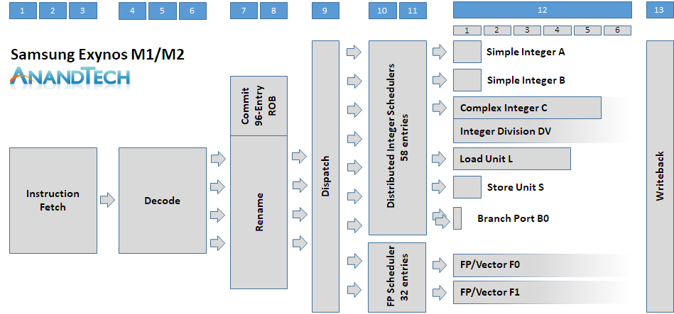
At heart the Exynos M1 and M2 microarchitectures are based on a 4-wide in-order stage for decode and dispatch. The wide decode stage was rather unusual at the time as ARM’s own Cortex A72 and A73 architectures made due with respectively 3 and 2-wide instruction decoders. With the Exynos M1/M2 being Samsung LSI’s first in-house microarchitecture it’s possible that the front-end wasn’t as advanced as ARM’s, as the latter’s 2-wide A73 microarchitecture was more than able to keep up in terms of IPC against the 4-wide M1 & M2. Samsung’s back-end for the M1 and M2 included 9 execution ports:
- Two simple ALU pipelines capable of integer additions.
- A complex ALU handling simple operations as well as integer multiplication and division.
- A load unit port
- A store unit port
- Two branch prediction ports
- Two floating point and vector operations ports leading to two mixed capability pipelines
The M1/M2 were effectively 9-wide dispatch and execution machines. In comparison the A73 dispatches up to 8 micro-ops into 7 pipelines and the A75 dispatches up to 11 µops into 8 pipelines, keeping in mind that we’re talking about very different microarchitectures here and the execution capabilities between the pipelines differ greatly. From fetch to write-back, the M1/M2 had a pipeline depth of 13 stages which is 2 stages longer than that of the A73 and A75, resulting is worse branch-misprediction penalties.
This is only a rough overview of the M1/M2 cores, Samsung published a far more in depth microarchitectural overview at HotChips 2016 which we’ve covered here.
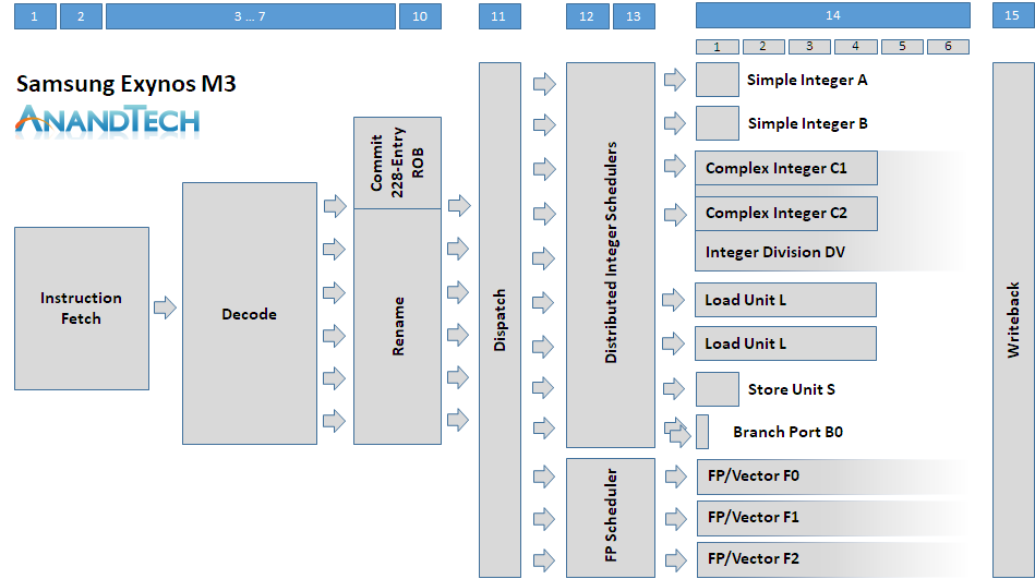
The Exynos M3 differs greatly from the M1/M2 as it completely overhauls the front-end and also widens the back-end. The M3 front-end fetch, decode, and rename stages now increases in width by 50% to accommodate a 6-wide decoder, making the new microarchitecture among one of the widest in the mobile space alongside Apple’s CPU cores.
This comes at a cost however, as some undisclosed stages in the front-end become longer by 2 cycles, increasing the minimum pipeline depth from fetch to writeback from 13 to 15 stages. To counteract this, Samsung must have improved the branch predictor, however we can’t confirm for sure what individual front-end stage improvements have been made. The reorder buffer on the rename stage has seen a massive increase from 96 entries to 228 entries, pointing out that Samsung is trying to vastly increase their ability to extract instruction level parallelism to feed their back-end execution units.
The depiction of the schedulers are my own best guess on how the M3 looks like, as it seemed to me like the natural progression from the M1 configuration. What we do know is that the core dispatches up to 12 µops into the schedulers and we have 12 execution ports:
- Two simple ALU pipelines for integer additions, same as on the M1/M2.
- Two complex ALUs handling simple integer additions and also multiplication and division. The doubling of the complex pipelines means that the M3 has now double the integer multiplication throughput compared to the M1/M2 and a 25% increase in simple integer arithmetic.
- Two load units. Again, the M3 here doubles the load capabilities compared to the M1 and M2.
- A store unit port, same as on the M1/M2.
- Two branch prediction ports, likely the same setup as on the M1/M2, capable of feeding the two branches/cycle the branch prediction unit is able to complete.
- Instead of 2 floating point and vector pipelines, the M3 now includes 3 of them, all of them capable of complex operations, theoretically vastly increasing FP throughput.
The simple ALU pipelines already operate at single-cycle latencies so naturally there’s not much room for improvement there. On the side of the complex pipelines we still see 4-cycle multiplications for 64-bit integers, however integer division has been greatly improved from 21 cycles down to 12 cycles. I’m not sure if the division unit reserves both complex pipelines or only one of them, but what is clear as mentioned before, integer multiplication execution throughput is doubled and the additional complex pipe also increases simple arithmetic throughput from 3 to 4 ADDs.
The load units have been doubled and their load latency remains 4 cycles for basic operations. The Store unit also doesn’t seem to change in terms of its 1-cycle latency for basic stores.
The floating point and vector pipelines have seen the most changes in the Exynos M3. There are 3 pipelines now with distributed capabilities between them. Simple FP arithmetic operations and multiplication see a three-fold increase in throughput as all pipelines now offer the capability, compared to only one for the Exynos M1/M2. Beyond tripling the throughput, the latency of FP additions and subtractions (FADD, FSUB) is reduced from 3 cycles down to 2 cycles. Multiplication stays at a 4-cycle latency.
Floating point division sees a doubling of the throughput as two of the three pipelines are now capable of the operations, and latency has also been reduced from 15 cycles down to 12 cycles. Cryptographic throughput of AES instruction doubles as well as two of the 3 pipelines are able to execute them. SHA instruction throughput remains the same. For simple vector operations we see a 50% increase in throughput due to the additional pipeline.

We’re only scratching the surface of what Samsung’s third-generation CPU microarchitecture is bringing to the table, but already one thing is clear: SLSI’s claim of doubling single-threaded performance does not seem farfetched at all. What I’ve covered here are only the high-level changes the in the pipeline configurations and we don’t know much at all about the improvements on the side of the memory subsystem. I’m still pretty sure that we’ll be looking at large increases in the cache sizes up to 512KB private L2’s for the cores with a large 4MB DSU L3. Given the floating point pipeline changes I’m also expecting massive gains for such workloads. The front-end of the M3 microarchitecture is still a mystery so here’s hoping that Samsung will be able to re-attend Hot Chips this year for a worthy follow-up presentation covering the new design.
With all of these performance improvements, it’s also expected that the power requirements of the core will be greatly beyond those of existing cores. This seems a natural explanation for the two-fold single-core performance increase while the multi-core improvement remains at 40% - running all cores of such a core design at full frequency would indeed showcase some very high TDP numbers.
If all these projections come to fruition, I have no idea how Samsung’s mobile division is planning to equalise the CPU performance between the Exynos 9810 and against an eventual Snapdragon 845 variant of the Galaxy S9, short of finding ourselves in a best-case scenario for ARM’s A75 vs a worst-case for the new Exynos M3. With 2 months to go, we’ll have to wait & see what both Samsung mobile and Samsung LSI have managed to cook up.


60 Comments
View All Comments
id4andrei - Wednesday, January 24, 2018 - link
A smartphone that cannot sustain its own performance is a flawed device. 50% throttle is not a feature, it is a band-aid aiming to avoid a total recall. We are talking about year old devices that get throttled with batteries that pass Apple's own diagnostics. No smartphone, laptop, tablet on this planet acts this way. It's the battery life that gets shorter and not the performance kneecapped.Around the 2 year mark, coincidently when the warranty expires(in Europe) the phone is throttled into oblivion. Directly, or indirectly if you wish, this IS planned obsolescence.
thunng8 - Thursday, January 25, 2018 - link
Throttle in 1 year? The 3 a10 devices in my household which are 15 months old hasn’t throttled and the a9 which is more than 2 years old hasn’t either.thunng8 - Thursday, January 25, 2018 - link
Not saying some users have seen throttling, but I have not seen in any phones that I have access to say so saying a blanket statement of throttle after 1 year and useless after 2 is ridiculous.id4andrei - Thursday, January 25, 2018 - link
The so called "fix" perhaps fleshes out the weaker combos. Your devices were less susceptible as they happened to have a sturdier battery.It's not useless per se, just a 40%-50% permanent penalty. All concealed, gaming warranty or insurance conditions. This is a cover up that plays exactly into planned obsolescence. Directly or indirectly, this is the effect.
thunng8 - Friday, January 26, 2018 - link
Like I said no penalty for my sisters 6s Plus which is close to 2.5 years old.I did tell her to get the battery replaced sometime this year as it’s cheap and she’ll be able to use it for at least another 2 years if not more.
NetMage - Monday, February 12, 2018 - link
So apparently all Android phones that throttle after 30 seconds should never have been sold ?name99 - Monday, February 19, 2018 - link
The GB4 numbers suggest that Samsung did indeed pull it off --- Integer IPC about 50% higher, so about A10 levels, and FP IPC (which is easier to boost) about90% higher, again A10 levels. Very impressive!In my defense at least part of that is surely due to precisely the various items I said were not covered by the article, from uncore (prefetch and cache quality) to front-end.
From recent LLVM activity we DO know, for example, that Samsung has become much more aggressive about instruction pairs they are willing to fuse (beyond the literals and compare+branch, they now have AES fusion, arithmetic followed by compare, and compare followed by selection).
Fusion is a great way to amplify the performance of your queues, and I think there still remains some performance to be squeezed out of fusion (especially now fusion of three successive instruction in the form of what are sometime called "chains"). Meaning that (IMHO) I don't see A11 levels of performance as the end of the road --- I expect Apple still to make meaningful improvement in bothe the A12 and A13. And it's nice to see that Samsung will likely be alongside them -- perhaps lagging by twelve to eighteen months, but providing enough pressure to keep Apple going.
(As for Intel which is already about 30% behind Apple in IPC, well...
I think in the Apple community we all pretty much hope that Samsung will move soon to shipping Exynos in laptops, putting more pressure for Apple to do the same, and soon enough [by 2020?] transitioning the Mac off x86.)
name99 - Tuesday, March 27, 2018 - link
Hmm. The full tests now https://www.anandtech.com/show/12520/the-galaxy-s9...suggest that my first instincts were correct, Samsung did NOT pull it off.
It's a shame we (still...) don't have comparable Apple numbers (eg SPEC2006) but both browser numbers and my tests regarding Wolfram Player suggest that Apple's performance advantage is broad and real, not limited to Geekbench.
As for Samsung? Did they optimize all structures ONLY for Geekbench? Do they run GB at unsustainable frequencies (ie good old fashioned benchmark detector cheating)? Or the slightly more subtle "run at frequencies that are stupid in terms of the energy/time tradeoff"?
Do they have a truly lousy DVFS scheduler?
Wardrive86 - Tuesday, January 23, 2018 - link
Excellent article again, thank you! That core diagram is beautiful -heart eyes-. I hope the drivers for their GPU has been enhanced as much as this CPU core has. Can't wait to see how it compares to the A75/Kryo 385Ej24 - Tuesday, January 23, 2018 - link
Can someone elaborate why Samsung doesn't equip US devices with exynos soc's? They did on the galaxy S6 and even used their own in house Shannon lte modem. The only reason I've read that they use Qualcomm in the US is because of the integrated modem in the snapdragon soc but it's clearly not necessary as the S6 stands testament to.