Intel Core with Radeon RX Vega M Graphics Launched: HP, Dell, and Intel NUC
by Ian Cutress on January 7, 2018 9:02 PM ESTNavigating Power: Intel’s Dynamic Tuning Technology
In the past few years, Intel has introduced a number of energy saving features, including advanced speed states, SpeedShift to eliminate high-frequency power drain, and thermal balancing acts to allow OEMs like Dell and HP to be able to configure total power draw as a function of CPU power requests, skin temperature, the orientation of the device, and the current capability of the power delivery system. As part of the announcement today, Intel has plugged a gap in that power knowledge when a discrete-class graphics processor is in play.
The way Intel explains it, OEMs that used separate CPUs and GPUs in a mobile device would design around a System Design Point (SDP) rather than a combined Thermal Design Power (TDP). OEMs would have to manage how that power was distributed – they would have to decide that if the GPU was on 100% and the SDP was reached, how the CPU and GPU would react if the CPU requested more performance.
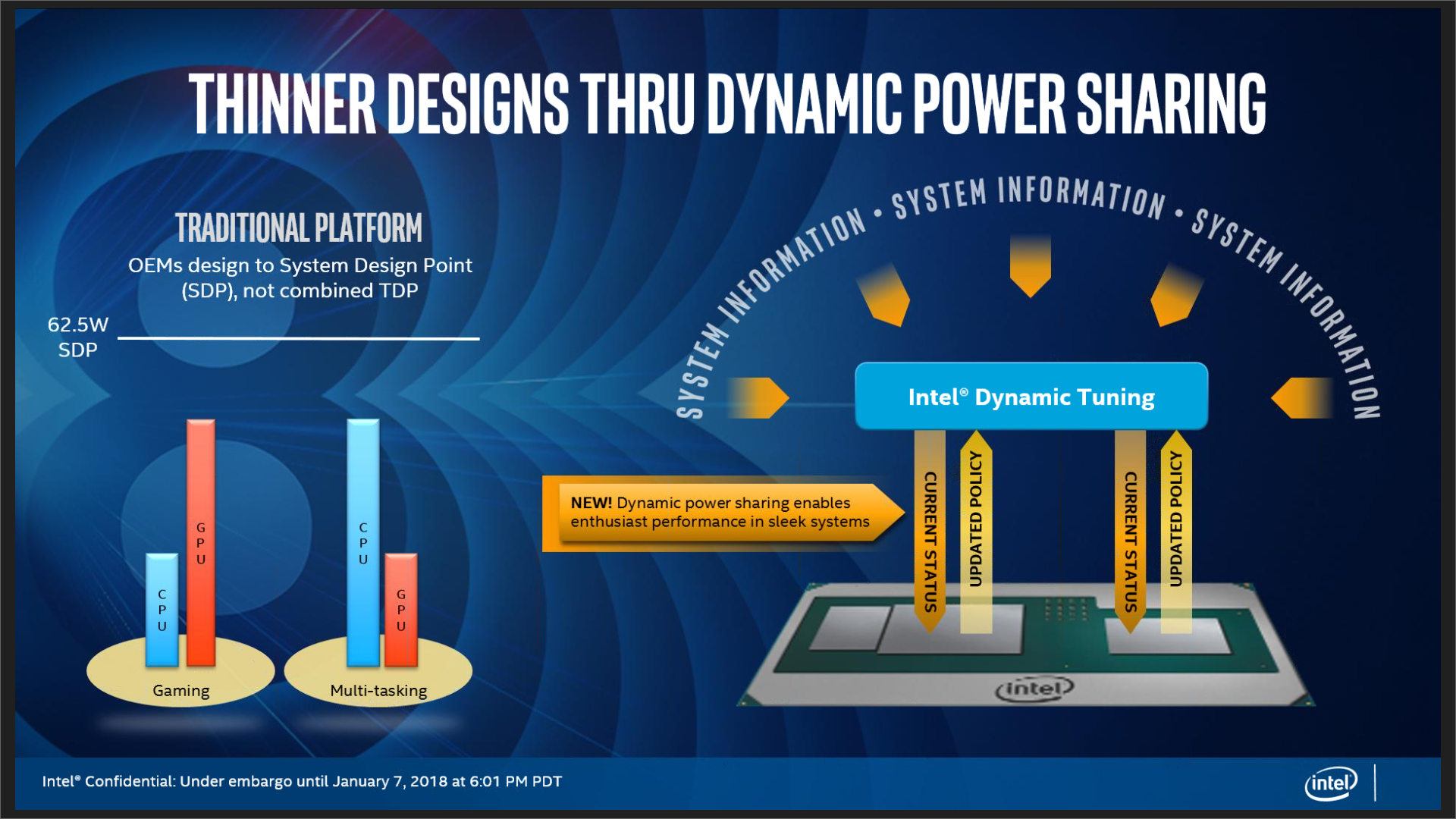
Intel’s ‘new’ feature, Intel Dynamic Tuning, leverages the fact that Intel can now control the power delivery mechanism of both the combined package, and distribute power to the CPU and pGPU as required. This leverages how Intel approached the CPU in response to outside factors – by using system information, the power management can be shared to maintain minimum performance levels and ultimately save power.
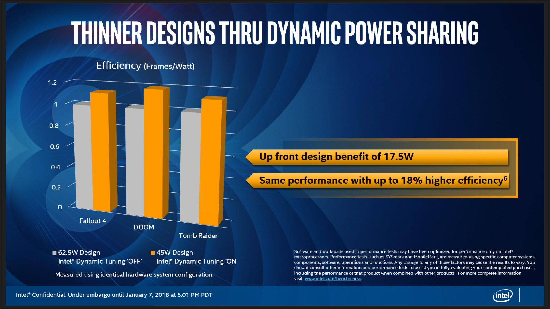
If that sounds a bit wishy-washy, it is because it is. Intel’s spokespersons during our briefing were heralding this as a great way to design a notebook, but failed to go into any sort of detail as to how the mechanism works, leaving it as a black box for consumers. They quoted that a design aiming at 62.5W SDP could have Intel Dynamic Tuning enabled and be considered a 45W device, and by managing the power they could also increase gaming efficiency up to 18% more frames per watt.
One of the big questions we had when Intel first starting discussing these new parts is how the system deals with power requests. At the time, AMD had just explained in substantial detail its methodology for Ryzen Mobile, with the CPU and GPU in the same piece of silicon, so it was a fresh topic in mind. When questioned, Intel wanted to wait until the official launch to discuss the power in more detail, but unfortunately all we ended up with was a high-level overview and a non-answer to a misunderstood question in the press-briefing Q&A.
We’re hoping that Intel does a workshop on the underlying technology and algorithms here, as it would help shine a light on how future Intel with Radeon designs are implementing their power budgets for a given cooling strategy.


66 Comments
View All Comments
skavi - Monday, January 8, 2018 - link
Do we even have 8th gen Y?evilpaul666 - Sunday, January 7, 2018 - link
So is this all Intel has for CES?extide - Sunday, January 7, 2018 - link
So, here we have a MCM with chips from three different fabs on it. 1 from Intel, 1 from GF, and one from Samsung or SKHynix.Have we ever seen something like that before?
Penti - Sunday, January 7, 2018 - link
So will we see a 24 CU Vega-chip with HBM2 as a discrete chip for laptops too? It's essentially designed as a lower tier RTG/AMD GPU, kinda specced like a replacement for Polaris 11.Cooe - Monday, January 8, 2018 - link
AMD announced Vega Mobile today which is pretty much exactly that. It's a freaking tiny package,and for that reason I expect it to be pretty successful vs Nvidia's traditional GDDR5 designs. (Though no word yet if the Vega Mobile and the semi-custom chip here are the same as far as CU count and what not, but it wouldn't be surprising).
Penti - Monday, January 8, 2018 - link
Same Z-height as KBL-G at least. Vega mobile was expected, is definitively related to the chip on the KBL-G package but might be a chip with a slightly different CU/SP count but renders make it look exactly the same.flashbacck - Sunday, January 7, 2018 - link
"Intel’s internal graphics, known as ‘Gen’ graphics externally, has been third best behind NVIDIA and AMD for grunt."Grunt? huh?
Holliday75 - Monday, January 8, 2018 - link
I thought the same thing.Kevin G - Sunday, January 7, 2018 - link
The one thing missing from this article, which I think if fair in the context of the fury of news last week, are Spectre and Meltdown. Intel is currently facing multiple law suits about it, especially in the context of bringing to market with a security flaw. These security flaws maybe the death blow to Cannon Lake which was originally to be a late 2018 part and already had the desktop parts removed form the line up in favor of Coffee Lake.There is another Lake part coming in late 2018 called Whiskey Lake and the rumors are pointing toward it being yet another Sky Lake based 14 nm part (see Kaby and Coffee Lake). I have no idea what these parts could provide other than potential fixes for Meltdown and Spectre minus the offhand possibility of an updated GPU. Next actual CPU core design is set to be Ice Lake which may also be their first 10 nm chip. Intel has shied away from doing to many firsts as once due to the difficulty of isolating problem (is it process? design? packaging? interconnect?) but Intel may have no choice.
Intel's CEO is set to take the stage at CES tomorrow so we'll probably get some answers to their roadmap as well has some groveling about Meltdown and Spectre.
Oh, for the curious, you can look up what codenames Intel does have the horizon here and see Whiskey Lake for yourselves:
https://www.intel.com/content/www/us/en/design/pro...
UtilityMax - Thursday, January 11, 2018 - link
This gotta be the worst time to announce a new Intel CPU. Sadly, I think the sheep that are the average consumers will gladly buy PCs with these CPUs.