NVIDIA Announces Tesla P100 Accelerator - Pascal GP100 Power for HPC
by Ryan Smith on April 5, 2016 3:15 PM EST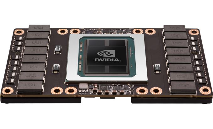
Today at their 2016 GPU Technology Conference, NVIDIA announced the first of their Pascal architecture powered Tesla cards, the Tesla P100. The P100 is the first major update to the Tesla HPC family since the launch of the first Kepler cards in late 2012, and represents a very sizable performance increase for the Tesla family thanks to the combination of the smaller 16nm manufacturing process and the Pascal architecture.
| NVIDIA Tesla Family Specification Comparison | ||||||
| Tesla P100 | Tesla K80 | Tesla K40 | Tesla M40 | |||
| Stream Processors | 3584 | 2 x 2496 | 2880 | 3072 | ||
| Core Clock | 1328MHz | 562MHz | 745MHz | 948MHz | ||
| Boost Clock(s) | 1480MHz | 875MHz | 810MHz, 875MHz | 1114MHz | ||
| Memory Clock | 1.4Gbps HBM2 | 5Gbps GDDR5 | 6Gbps GDDR5 | 6Gbps GDDR5 | ||
| Memory Bus Width | 4096-bit | 2 x 384-bit | 384-bit | 384-bit | ||
| Memory Bandwidth | 720GB/sec | 2 x 240GB/sec | 288GB/sec | 288GB/sec | ||
| VRAM | 16GB | 2 x 12GB | 12GB | 12GB | ||
| Half Precision | 21.2 TFLOPS | 8.74 TFLOPS | 4.29 TFLOPS | 6.8 TFLOPS | ||
| Single Precision | 10.6 TFLOPS | 8.74 TFLOPS | 4.29 TFLOPS | 6.8 TFLOPS | ||
| Double Precision | 5.3 TFLOPS (1/2 rate) |
2.91 TFLOPS (1/3 rate) |
1.43 TFLOPS (1/3 rate) |
213 GFLOPS (1/32 rate) |
||
| GPU | GP100 (610mm2) |
GK210 | GK110B | GM200 | ||
| Transistor Count | 15.3B | 2 x 7.1B(?) | 7.1B | 8B | ||
| TDP | 300W | 300W | 235W | 250W | ||
| Cooling | N/A | Passive | Active/Passive | Passive | ||
| Manufacturing Process | TSMC 16nm FinFET | TSMC 28nm | TSMC 28nm | TSMC 28nm | ||
| Architecture | Pascal | Kepler | Kepler | Maxwell 2 | ||
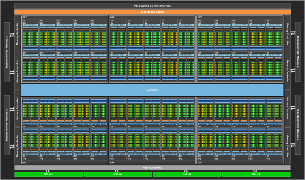
Powering the Tesla P100 is a partially disabled version of NVIDIA's new GP100 GPU, with 56 of 60 SMs enabled. GP100 is a whale of a GPU, measuring 610mm2 in die size on TSMC's 16nm FinFET process and composed of 15.3B transistors. It is remarkable in and of itself that NVIDIA and TSMC are in volume production of such a large 16nm die at this time, as everything else we've seen with a confirmed size is at best one-quarter of this size. GP100 is being produced on TSMC's Chip-On-Wafer-On-Substrate technology, with this line apparently being used for putting the GPU and HBM2 DRAM stacks on the same interposer.
We'll dive into the full Pascal architecture (as implemented by GP100) at a later time, but it's worth noting that Pascal here is 64 FP32 CUDA cores per SM, versus 128 on Maxwell. Each of those SMs also contains 32 FP64 CUDA cores - giving us the 1/2 rate for FP64 - and new to the Pascal architecture is the ability to pack 2 FP16 operations inside a single FP32 CUDA core under the right circumstances. With a boost clock of 1.48GHz, altogether Tesla P100 will offer 10.6 TFLOPS of FP32 performance or 5.3 TFLOPS of FP64 performance, more than doubling and tripling Tesla K40's rated throughput on these metrics respectively. NVIDIA has been happy to crow about the performance of Tesla P100, and for good reason, as this stands to be a very powerful processor.
Paired with the GP100 GPU on Tesla P100 is 16GB of HBM2 VRAM, laid out in 4 stacks for a 4096-bit memory bus. NVIDIA quotes P100 as offering 720GB/sec of memory bandwidth, which works out to a memory clock of 1.4Gbps. As we've seen with other HBM products, this marks a significant increase in memory bandwidth, more than doubling NVIDIA's last generation of cards.
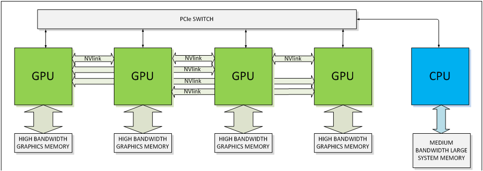
In their announcement, NVIDIA also confirmed that Tesla P100 will support NVLink, with 4 NVLink controllers. Previously announced, NVLink will allow GPUs to connect to either each other or to supporting CPUs (OpenPOWER), offering a higher bandwidth cache coherent link than what PCIe 3 offers. This link will be important for NVIDIA for a number of reasons, as their scalability and unified memory plans are built around its functionality.
Speaking of functionality, Tesla P100 and the underlying GP100 GPU is a full-featured HPC GPU. It supports all of the HPC-centric functionality that the Tesla K20/40/80 embodied, including ECC memory protection for the register file, caches, and HBM2 DRAM. Coupled with the very high FP64 rate, and it's clear that this is the successor of the GK110/GK210 GPU.

NVIDIA's pictures also confirm that this is using their new mezzanine connector, with flat boards no longer on perpendicular cards. This is a very HPC-centric design (I'd expect to see plenty of PCIe cards in time as well), but again was previously announced and is well suited for the market NVIDIA is going after, where these cards will be installed in a manner very similar to LGA CPUs. The P100 is rated for a TDP of 300W, so the cooling requirements are a bit higher than last-generation cards, most of which were in the 230W-250W range.
Finally, in its initial implementation NVIDIA is focusing on customers that need extreme scaling capabilities, and I wouldn't be too surprised if this was in part due to the margins of that market and how these initial cards will be in demand. NVLink of course plays a big part here, with NVIDIA able to go up to 8-way configurations thanks to it.


Source: NVIDIA


93 Comments
View All Comments
extide - Thursday, April 7, 2016 - link
Well, mobile SoC's don;t technically use 3d stacking, because they don't use TSV's or microbumps, but they uses PoP, which is Package on Package, where it's just the memory package (die in packaging, not bare die like 3d stack would be) on top of the SoC package with regular BGA balls connecting them. They might possibly move to a true 3d stack in the future. Yes PoP is technically a "3d" stack, but the term 3d stack has a specific meaning in this case.Fusion_GER - Tuesday, April 5, 2016 - link
First GPU using GPC and TPC (TPC was gone since the GTX480)Fusion_GER - Tuesday, April 5, 2016 - link
http://www.anandtech.com/show/2549/2T1beriu - Tuesday, April 5, 2016 - link
To all the people saying that consumer dies will have less DP cores, no NVLink, no HBM or many other things ripped out of its dies, I want to remind you that NVIDIA gave just one codename for its 2016 architecture release - Pascal.So many architecture changes would ask for a different codename. Volta coming in 2018.
dragonsqrrl - Tuesday, April 5, 2016 - link
Did anyone suggest different dies would used? Everything discussed including FP64 ratios and NVLink can be accomplished through binning or some method other than manufacturing differentvFunct - Tuesday, April 5, 2016 - link
FP ratios aren't changed by binning. That's intrinsic to the design.dragonsqrrl - Tuesday, April 5, 2016 - link
FP64 cores can be fused off. Clocks can also be limited to effect the ratio.Michael Bay - Thursday, April 7, 2016 - link
What would be the point of having NVLink on consumer videocard if no chipset provider supports it?T1beriu - Thursday, April 7, 2016 - link
Consumer dies always had extra bits disabled that were enabled in professional dies. NVLink will be disabled.extide - Thursday, April 7, 2016 - link
NVLink will not be used on the consumer cards, there is no point.