Testing Samsung 850 Pro Endurance & Measuring V-NAND Die Size
by Kristian Vättö on July 7, 2014 1:20 PM ESTV-NAND Die Size: Bigger Than What We Initially Thought
In our 850 Pro review, I did some calculations to estimate the die size of the second generation V-NAND based on the first generation V-NAND. As some of our clever readers pointed out, the die size does not scale perfectly with the die capacity because the peripheral circuitry cannot be scaled as aggressively as the capacity can be. As a result, my initial estimation ended up being way too small because I did not take the scaling of the peripheral circuitry into account.
Unfortunately, Samsung would not disclose the die size during the Q&A at the SSD Global Summit so I had to seek for an alternative way to figure out the correct die size. In the showroom, Samsung had the second generation 32-layer V-NAND wafer, which actually gives us everything we need to calculate a fairly accurate estimation of the die size.
The picture on top shows what the wafer looks like. It does not look any different from the typical 2D NAND wafer, which should not be a surprise given that the change happened deep inside. And no, the V-NAND wafer is not thicker than any normal wafer (at least not by eye) because the V-NAND stack is still in the order of microns.
As for the die size, I calculated 44 dies in the vertical direction, which means that with a 300mm wafer the depth of a single die is approximately 6.8mm.
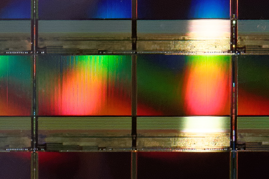
Courtesy of PC Perspective
To figure out the width of the die, you can either count the dies in the horizontal direction or go with the lazy route and just calculate the proportion of the depth and width. Allyn Malventano from PC Perspective was able to grab this awesome photo of the die itself, so I used the ruler tool in Photoshop to measure the size of the die along both X and Y axes and it appears that the width of the die is about 2.05 times its depth (note that it is a two-plane design). In other words, the die size is around 6.8mm x 14.0mm, which works out to be 95.4mm2.
| NAND Die Comparison | ||||
| Samsung 1st Gen V-NAND | Samsung 2nd Gen V-NAND | Micron 16nm NAND | Toshiba A19nm NAND | |
| Die Capacity | 128Gbit | 86Gbit | 128Gbit | 64Gbit |
| Die Size | 133mm2 | ~95.4mm2 | 173mm2 | 94mm2 |
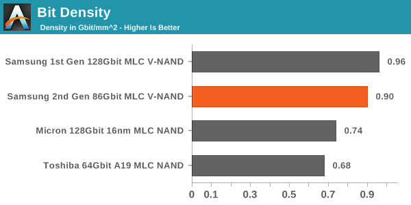
Here is an updated bit density graph. Even with the updated, larger die size, V-NAND is noticeably denser than 2D NAND, although the first generation appears to be more dense. I am guessing the smaller die size is better for yields (larger chips have higher probability of manufacturing errors), which makes the second generation more cost efficient despite the slightly lower density.


39 Comments
View All Comments
sovanbu - Monday, July 7, 2014 - link
Glad I still have 20 days to return the 840 Pro I bought. This will be much faster and more reliable.Solid State Brain - Monday, July 7, 2014 - link
Interesting test. A bit disappointing that the NAND on this drive is officially "only" rated for 6000 P/E cycles. Not that it's going to ever be a problem for most users, even likely most of those dealing with video editing (often involving a large amount of writes, but usually of sequential nature - meaning low write amplification), also given Samsung's client environment scenario policy on its 10 year warranty for this drive.I'm assuming that to obtain a 11x worst case write amplification you hammered the drive with sustained writes raw to the drive (bypassing the OS), am I correct? During normal or even intense usage with typical pro/consumer workloads I think it would be very difficult for users to observe such a high value, with TRIM and garbage collection algorithms sorting out data on the NAND. I also guess that people who consciously write a huge amount of data will want to increase the overprovisioning area for performance and NAND endurance reasons.
Speaking of which, it would be interesting to find out how much of an effect increasing OP has in decreasing worst case write amplification.
Kristian Vättö - Monday, July 7, 2014 - link
Yes, I tested with a raw drive. Like I said, it's a worst-case scenario that may apply to some write intensive enterprises -- client workloads, even heavy ones, don't usually exceed queue depth of 5 anyway.I'll probably run some more in depth write amplification tests including playing with the over-provisioning for the enterprise review of the 850 Pro, assuming I manage to find the time for all that :)
mapesdhs - Monday, July 7, 2014 - link
What do you mean by 'much' faster? And as for more reliable, it's usually more risky to
adopt a totally new SSD. Besides, the 830/840/EVO/840-Pro series are all reliable models,
so how have you quantified what 'more' reliable will mean when it's a new SSD vs. existing
models that have already gone through the hunt for bugs to be ironed out, with consequent
fw updates issued?
In reality, I highly doubt you'd ever notice the difference between a 256GB 840 Pro and a
256GB 850 Pro.
Ian.
wintermute000 - Monday, July 7, 2014 - link
Normal desktop/laptop user agreed but there are people with more demanding requirements.....mapesdhs - Tuesday, July 8, 2014 - link
Demanding in what way? For something so demanding that an 840 Pro isn't enough,
one ought to be using an Enterprise model instead.
Ian.
extide - Wednesday, July 9, 2014 - link
You know, the thing about this SSD is that it uses the same controller as the 840 EVO, which would mean it uses very similar firmware as the 840 EVO. Of course, you may see some changes in the FW related to the fact that the V-NAND has greater abilities, but most of the firmware should be pretty much the same. So, same controller, similar firmware, and new flash. So, it's really not too bad, and I would definitely trust it more than a drive from, say... a brand new series, with a new controller, and maybe even a radically different interface or protocol, or even a brand new/unknown company!Mark_gb - Wednesday, July 9, 2014 - link
It will be so much faster that you wont even notice the difference... LOLIt will probably last a lot longer than your 840 Pro, but even that is a crap shoot. Your 840 Pro could last another 10 years, or the 850 could die the second day you use it.
jjj - Monday, July 7, 2014 - link
"I am guessing the smaller die size is better for yields (larger chips have higher probability of manufacturing errors), which makes the second generation more cost efficient despite the slightly lower density. "You have more layers for the second gen and that impacts both yield and cost so you can't make that kind of assumption.
Maybe you should have also compared density on a per layer basis ,the difference seems quite huge then between the 2 gens.
Kristian Vättö - Monday, July 7, 2014 - link
You are right that having more layers impacts yield and production cost but it does not refute the fact that the die size affects yield as well. There must be something in 2nd Gen V-NAND to make it more cost efficient than the first Gen because otherwise it makes absolutely no sense. It's not denser because the array efficiency is significantly lower thanks to the lower capacity, so the only thing I can think of is higher yield thanks to the smaller die size.What do you mean by "density on a per layer basis"? The cell size should have remained the same because it is still a 40nm process with no change in equipment, meaning that the second Gen simply adds more layers.