FIC AD11 Socket-A AMD 760 DDR ATX
by Anand Lal Shimpi on February 13, 2001 1:57 AM EST- Posted in
- Motherboards
Tweaking made easy
Regardless of how you paint the picture, this is an enthusiast's market. Because it is so, tweaking and overclocking are two very important issues when looking at any motherboard. We have recently been devoting quite a bit of time to covering the KT133A based solutions and have found them to be quite tweak-friendly, can the same be said about AMD 760 based motherboards? As far as the FIC AD11 is concerned, you can put your fears to rest as there are quite a few settings the AD11 let's you configure on your own to get the most out of your system.
As we outlined in our Socket-A Overclocking Guide, multiplier adjustment is key to getting the most effective overclock out of your processor. Just as the AZ11 had the multiplier adjustment circuitry already on the board, the same was true for the AD11 we looked at last September. In the shipping revision of the AD11, what we are looking at today, FIC implements clock multiplier adjustment through a set of dipswitches called the ADR switch, allowing values from 5.0x to 12.5x. In order to take advantage of these adjustable ratios you will first need to unlock your CPU, and then set a jumper to enable the dipswitch settings.
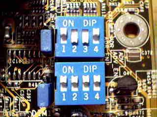
The two sets of dipswitches: ADR and ADV
The more you push your CPU, the more tolerance levels become an issue. One way to combat this is by simply increasing the voltage supplied to your processor. The voltage itself won't harm your CPU (as long as you remain within AMD's specified operating range) however the same can't be said for the added heat/stress caused by overclocking. For anyone that has had any experience overclocking, a decent voltage boost doesn't generally result in permanent CPU damage however we take no responsibility for any of the after effects; neither does FIC. In order to offer the ability to do so, FIC does provide another set of switches, called the ADV switch that allow you to select from the following list of core voltage settings: 1.475 / 1.700 / 1.725 / 1.750 / 1.775 / 1.800 / 1.825 / 1.850 V. Like the multiplier settings, these core voltage options must be set from the dipswitches and there is no utility in the BIOS to do this for you.
The available FSB settings are somewhat disappointing for the AD11. The available FSB frequencies that are offered are: 100 / 103 / 105 / 110 / 113 / 117 / 133 / 138 / 140 / 144 and 150MHz. Unfortunately this results in quite a few large jumps between FSB frequencies, which can be the limiting factor in FSB overclocking. As shown in our overclocking tests, we were able to push the FSB speed to 140MHz without a hitch. However at 144MHz, the system passed the POST but wasn’t able to locate the boot sector of the hard drive correctly and failed to load Windows. This was probably a limit of the DDR SDRAM being used or a combination of that and the board itself. Remember that a 11MHz increase in FSB frequency translates into an effective 22MHz increase because you're dealing with DDR front side and memory buses. We know the limitation doesn't exist with the FSB since we have gotten KT133A boards up higher than 140MHz, leaving the DDR SDRAM as the major culprit here. In the end, the smaller the FSB increments you have, the more precise overclocking you can do since the system may have been just fine at 142MHz but not 144MHz.
We came across a very interesting anomaly during our testing of the AD11. Because the AGP clock divider must change depending on whether you are running at the 100MHz or 133MHz FSB (AGP clock = 66MHz = FSB * 2/3 or FSB / 2) there is a jumper that selects 100 or 133MHz FSB operation (the jumper really just selects the AGP ratio and enables the FSB speeds accordingly). However, for each setting, you are able to choose the entire range of FSB speeds in the BIOS, and that creates some problems. During our testing, initially we had the jumper set to 100MHz and ran the CPU at 100MHz flawlessly. Then we turned off the system, set the jumper to 133MHz, reduced the multiplier ratio from 10 to 7.5, and the system didn’t POST at all.
In the end we discovered that the problem was related to the FSB speeds in the BIOS and the jumper states. Before you change the jumper from 100MHz to 133MHz, you will have to go into the BIOS and change the FSB speed to 133MHz and reboot. The reboot will fail and board won't POST. Next, you have to turn off your system, and manually change the jumper to 133MHz. Now boot up the system and it will run at 133MHz without a hitch. Moving back from 133MHz to 100MHz requires the same process. This is entirely too much work to do what should simply be manipulation of a single setting either in the BIOS or on the motherboard. Hopefully FIC will address this issue with a future BIOS update.
Speaking of BIOS functions, there are a number of memory tweaking options that are present within the AD11's BIOS setup. The most influential setting being the CAS Latency which our test DDR SDRAM DIMM allowed us to run at a setting of 2 instead of 2.5 which was what we were limited to when we first looked at the AD11.
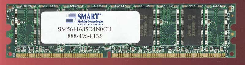
Smart Modular Technologies 128MB PC2100 CAS2 DDR SDRAM module


0 Comments
View All Comments