NVIDIA Launches Tesla K20 & K20X: GK110 Arrives At Last
by Ryan Smith on November 12, 2012 9:00 AM ESTGK110: The GPU Behind Tesla K20
Now that we’ve discussed the Telsa K20 series from the big-picture perspective of performance, configurations, pricing, and the marketplace, we can finally dive into the technical underpinnings of the K20.
Announced alongside the Tesla K20 back at NVIDIA’s GTC 2012 was the GPU that would be powering it: GK110. In a reversal of their usual pattern, GK110 was to be NVIDIA’s first compute-oriented Kepler GPU (GK10X having been significantly stripped for gaming efficiency purposes), but it would be the last Kepler GPU to launch. Whereas in the Fermi generation we saw GF100 first and could draw some conclusions about the eventual Tesla cards from that, GK110 has been a true blank slate. On the other hand because it builds upon NVIDIA’s earlier Kepler GPUs, we can draw a clear progression from GK104 to GK110.
GK110 is NVIDIA’s obligatory big-die GPU. We don’t have a specific die size, but at 7.1 billion transistors it is now the biggest GPU ever built in terms of transistors, dwarfing the 3.5B transistor GK104 and the 4.3B transistor Tahiti GPU from AMD. These big-die GPUs are unwieldy from a fabrication and power consumption perspective, but the end result is that the performance per GPU is unrivaled due to the fact that so many tasks (both graphical and compute) are embarrassingly parallel and map well to the large arrays of streaming processors found in a GPU.
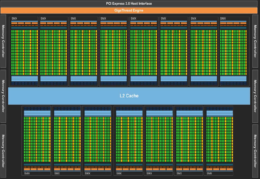
Like GF100 before it, GK110 has been built to fill multiple roles. For today’s launch we’re mostly talking about it from a compute perspective – and indeed most of the die is tied up compute hardware – but it also has all of the graphics hardware we would expect in an NVIDIA GPU. Altogether it packs 15 SMXes and 6 ROP/L2/memory controller blocks, versus 8 SMXes and 4 ROP/L2/memory blocks on GK104. Not accounting for clockspeeds this gives GK110 87% more compute performance and 50% more memory bandwidth than GK104. But there’s a great deal more to GK110 than just a much larger collection of functional units.
| NVIDIA GPU Comparison | ||||||
| Fermi GF100 | Fermi GF104 | Kepler GK104 | Kepler GK110 | |||
| Compute Capability | 2.0 | 2.1 | 3.0 | 3.5 | ||
| Threads/Warp | 32 | 32 | 32 | 32 | ||
| Max Warps/SM(X) | 48 | 48 | 64 | 64 | ||
| Max Threads/SM(X) | 1536 | 1536 | 2048 | 2048 | ||
| Register File | 32,768 | 32,768 | 65,536 | 65,536 | ||
| Max Registers/Thread | 63 | 63 | 63 | 255 | ||
| Shared Mem Config |
16K 48K |
16K 48K |
16K 32K 48K |
16K 32K 48K |
||
| Hyper-Q | No | No | No | Yes | ||
| Dynamic Parallelism | No | No | No | Yes | ||
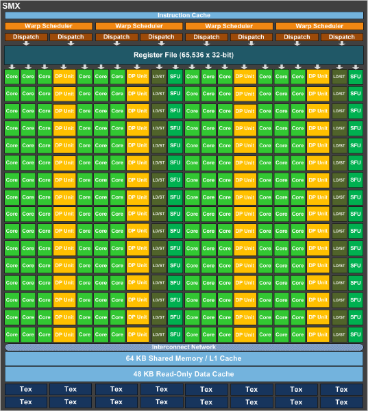
Fundamentally GK110 is a highly enhanced if not equally specialized version of the Kepler architecture. The SMX, first introduced with GK104, is the basis of GK110. Each GK104 SMX contained 192 FP32 CUDA cores, 8 FP64 CUDA cores, 256KB of register file space, 64KB of L1 cache, 48KB of uniform cache. In turn it was fed by 4 warp schedulers, each with two dispatch units, allowing GK104 to issue instructions from warps in a superscalar manner.
GK110 SMX
GK110 builds on that by keeping the same general design, but tweaking it for GK110’s compute-focused needs. The single biggest change here is that rather than 8 FP64 CUDA cores GK110 has 64 FP64 CUDA cores, giving it 8 times the FP64 performance of a GK104 SMX. The SMXes are otherwise very similar at a high level, featuring the same 256KB of register file space, 64KB of L1 cache, 48KB of uniform cache, and the same warp scheduler structure. This of course does not include a number of low level changes that further set apart GK104 and GK110.
Meanwhile this comparison gets much more jarring if we take a look at GK110 versus GF100 and by extension Tesla K20 versus its direct predecessors, the Fermi based Tesla family. The GK110 SMX compared to the GF100 SM is nothing short of a massive change. Superficially NVIDIA has packed many more CUDA cores into an SMX than they have an SM due to the change from a shader design that ran fewer CUDA cores at a very high (double pumped) clockspeed to a design that runs many more CUDA cores at a lower (single pumped) clockspeed, but they also have changed their warp execution model on its head in the process.

GF100/GF110 SM
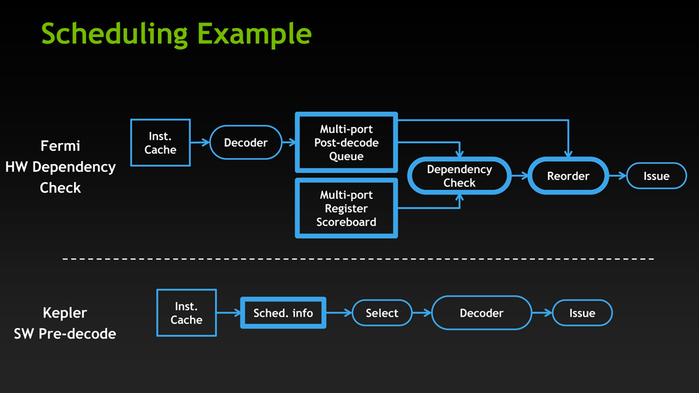
GF100 was essentially a thread level parallelism design, with each SM executing a single instruction from up to two warps. At the same time certain math instructions had variable latencies, so GF100 utilized a complex hardware scoreboard to do the necessary scheduling. Compared to that, GK110 introduces instruction level parallelism to the mix, making the GPU reliant on a mix of high TLP and high ILP to achieve maximum performance. The GPU now executes from 4 warps, ultimately executing up to 8 instructions at once if all of the warps have ILP-suitable instructions waiting. At the same time scheduling has been moved from hardware to software, with NVIDIA’s compiler now statically scheduling warps thanks to the fact that every math instruction now has a fixed latency. Finally, to further improve SMX utilization FP64 instructions can now be paired with other instructions, whereas on GF100 they had to be done on their own.
The end result is that at an execution level NVIDIA has sacrificed some of GF100’s performance consistency by introducing superscalar execution – and ultimately becoming reliant on it for maximum performance. At the same time they have introduced a new type of consistency (and removed a level of complexity) by moving to fixed latency instructions and a static scheduled compiler. Thankfully a ton of these details are abstracted from programmers and handled by NVIDIA’s compiler, but for HPC users who are used to getting their hands dirty with low level code they are going to find that GK110 is more different than it would seem at first glance.
With that said, even with the significant changes to their warp execution model, GK110 brings more changes yet. We can’t hope to replicate the sheer amount of depth NVIDIA’s own GK110 whitepaper covers, but there are several other low-level changes that further separate GK110 from GF100.
Space and bandwidth for both the register file and the L2 cache have been greatly increased for GK110. At the SMX level GK110 has 256KB of register file space, composed of 65K 32bit registers, as compared to 128KB of such space (32K registers) on GF100. Bandwidth to those register files has in turn been doubled, allowing GK110 to read from those register files faster than ever before. As for the L2 cache, it has received a very similar treatment. GK110 uses an L2 cache up to 1.5MB, twice as big as GF110; and that L2 cache bandwidth has also been doubled.
What makes this all the more interesting is that while NVIDIA significantly increased the number of CUDA cores in an SM(X), in fact by far more than the increase in cache and register file sizes, they only marginally increased the number of threads that are actually active on an SMX. Each GK110 SMX can only have up to 2K threads at any time, 1.33x that of GF100 and its 1.5K threads. So as a result GK110 is working from a thread pool only slightly larger than what GF100 worked with, which means that despite the increase in CUDA cores they actually improve their performance in register-starved scenarios as there are more registers available to each thread. This goes hand in hand with an increase in the total number of registers each thread can address, moving from 63 registers per thread on GF100 to 255 registers per thread with GK110.
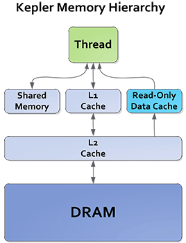
While we’re on the subject of caches, it’s also worth noting that NVIDIA has reworked their texture cache to be more useful for compute. On GF100 the 12KB texture cache was just that, a texture cache, only available to the texture units. As it turns out, clever programmers were using the texture cache as another data cache by mapping normal data at texture data, so NVIDIA has promoted the texture cache to a larger, more capable cache on GK110. Now measuring 48KB in size, in compute mode the texture cache becomes a read-only cache, specializing in unaligned memory access patterns. Furthermore error detection capabilities have been added to it to make it safer for use with workloads that rely on ECC.
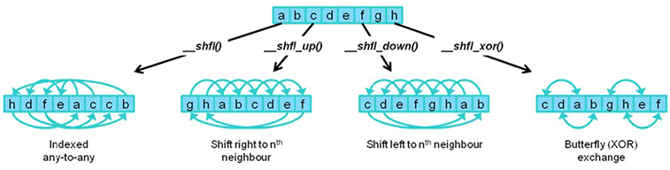
Last, but certainly not least in our low level look, NVIDIA has added a number of new instructions and operations to GK110 to further improve performance. New shuffle instructions allow for threads within a warp to share (i.e. shuffle) data without going to shared memory, making the process much faster than the old load/share/store method. Meanwhile atomic operations have also been overhauled, with NVIDIA both speeding up the execution speed of atomic operations and adding some FP64 operations that were previously only available for FP32 data.


73 Comments
View All Comments
kwrzesien - Monday, November 12, 2012 - link
My first First! Okay, now back to work.DigitalFreak - Monday, November 12, 2012 - link
I wouldn't call riding the short-bus work...kwrzesien - Monday, November 12, 2012 - link
Hey, I wouldn't call reading news work either!CeriseCogburn - Thursday, November 29, 2012 - link
Thank you insane amd fanboys, for months on end, you've been screaming that nVidia yields are horrible and they're late to the party, while nVidia itself has said yields are great, especially in the GPU gaming card space.now the big amd fanboy lie is exposed.
" Interestingly NVIDIA tells us that their yields are terrific – a statement backed up in their latest financial statement – so the problem NVIDIA is facing appears to be demand and allocation rather than manufacturing."
(that's in the article above amd fanboys, the one you fainted...after raging... trying to read)
Wow.
I'm so glad this site is so fair, and as we see, as usual, what nVidia has been telling them is considered a lie for a very, very long time, until the proof that it was and is actually the exact truth and has been all along is slammed hard into the obstinate amd fan brain.
So nVidia NEVER had an ongoing yield issue on 600 series..
That's what they said all along, and the liars, knows as amd fanboys, just lied instead, even after they were informed over and over again that nVidia did not buy up a bunch of manufacturing time early.
Thanks amd fanboys, months and months of your idiot lies makes supporting amd that much harder, and now they are truly dying.
Thank you for destroying competition.
mayankleoboy1 - Monday, November 12, 2012 - link
Anand, I am a Nvidia fanboi.But still i was surprised by your AMD S10000 coverage. That merited a page in the _pipeline_ section.
And a product from Nvidia gets a front seat, _3 page_ article ?
Bias, or page hits ?
Ryan Smith - Monday, November 12, 2012 - link
I had more to write about the K20, it's as simple as that. This is the first chance I've had to write in-depth about GK110, whereas S10000 is a dual-chip board using an existing GPU.lx686x - Monday, November 12, 2012 - link
Ohhh the W9000/8000 review that never got a promised part 2? And the S9000 and S7000 that was also thrown in the pipeline?tviceman - Monday, November 12, 2012 - link
Just like the gtx650 that never got it's own review. Get over it.lx686x - Monday, November 12, 2012 - link
It wasn't promised, get over it.The Von Matrices - Tuesday, November 13, 2012 - link
It was promised, but it never was published.http://www.anandtech.com/show/6289/nvidia-launches...
"We’ll be looking at the GTX 650 in the coming week, at which point we should have an answer to that question."