MIPS Technologies Updates Processor IP Lineup with Aptiv Series
by Ganesh T S on May 10, 2012 8:55 AM ESTThe proAptiv family of processors can contain 1 to 6 proAptiv cores, each of which implements in about half the size of a standard Cortex-A15 core. This is not entirely impossible, given that some people in the industry feel that ARM's Cortex-A15 implementation takes up too much area for the advertised performance. However, it is likely that the NEON engine is being accounted for in the Cortex-A15 area while the proAptiv implementation doesn't take into account the 32 bit SIMD engine (DSP ASE). [ Update: MIPS clarified that the DSP ASE is not a configurable block and is included in the quoted area. The precise area numbers for ARM are estimates only, since ARM has published no concrete specifications for the Cortex-A15. MIPS also attempted to remove the estimated area for NEON, with the desire to achieve as close to an “apples to apples” comparison in area as possible].
The proAptiv core is a superscalar out-of-order CPU with quad instruction fetch and fused triple dispatch. In the absence of any dependencies, the CPU can issue up to four integer and two floating point operations. Multi-level TLBs and branch target buffers / sophisticated branch prediction aid in getting more than 60% better performance over the previous generation 1074K series. The FPU is dual issue and runs at the same speed as the CPU.
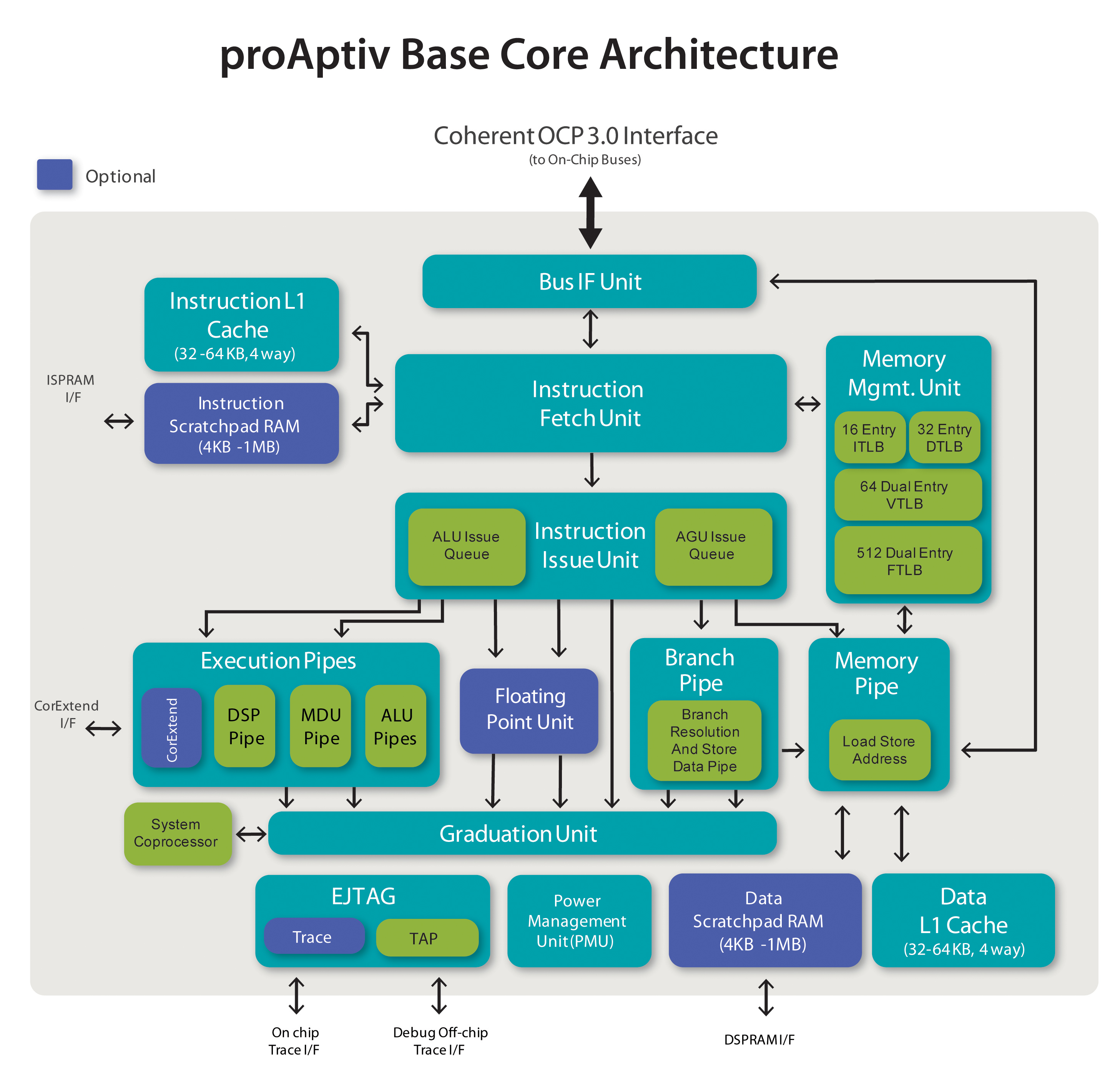
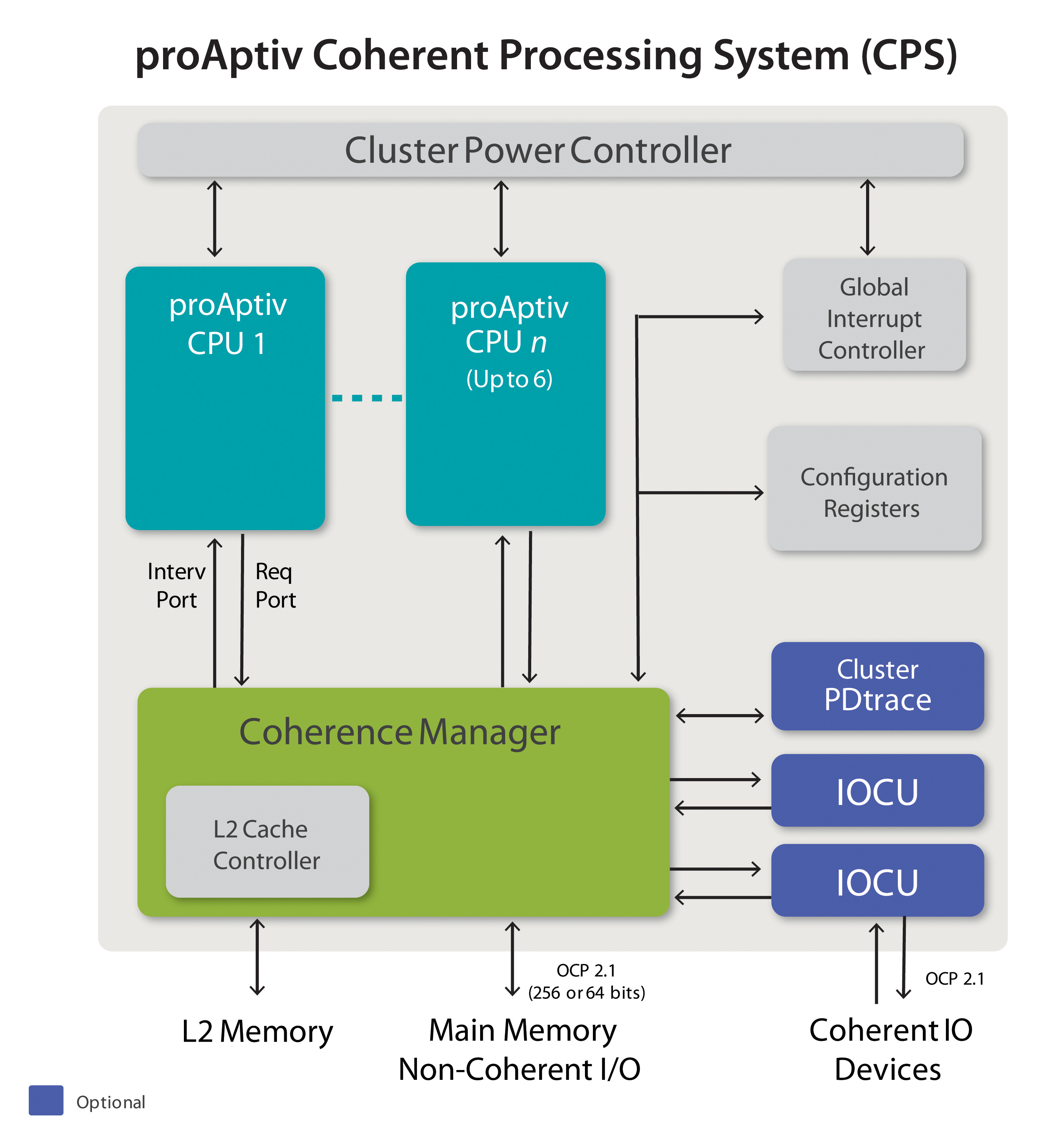
The proAptiv and interAptiv families implement EVA (Extended Virtual Addressing) in order to better utilize the available address space. Similar to the Cortex-A15, the IP includes a coherence manager and an integrated L2 cache controller with ECC support. While Cortex-A15 supports up to 32 cores, the proAptiv family supports up to 6. An interesting aspect of the Coherent Processing System (CPS) is the presence of a cluster power controller which does clock gating per core (common in other multi-core CPUs also) and voltage domain / gating per core. The latter has interesting applications in scenarios similar to ARM's big:LITTLE architecture. Instead of tying up a big core such as the A15 with a smaller one like the A7, MIPS suggests that licensees could implement a multi-core proAptiv system with some cores running at much lower frequencies / lower voltage to save upon power (since the proAptiv cores are already small compared to the A15 core).
| Architecture Comparison | |||||||||
| proAptiv | ARM Cortex A9 | Qualcomm Krait | ARM Cortex A15 | ||||||
| Decode | 3-wide | 2-wide | 3-wide | 3-wide | |||||
| Pipeline Depth | 13 stages | 8 stages | 11 stages | 15 stages | |||||
| Out of Order Execution | Y | Y | Y | Y | |||||
| Pipelined FPU | Y | Y | Y | Y | |||||
| SIMD / Media Processing Engine | DSP ASE (32-bit wide) | Optional MPE (64-bit wide) | Y (128-bit wide) | Optional MPE (128-bit wide) | |||||
| Process Technology | 40nm / 28nm | 40nm / 32nm | 28nm | 28nm | |||||
| Typical Clock Speeds | 1.2GHz* | 1.2GHz | 1.5GHz | 2.5GHz | |||||
While ARM expects the A15 to reach up to 2.5 GHz in the HP/G processes, MIPS only expects up to 1.5 GHz. That said, embedded applications using the proAptiv are likely to be power sensitive, and while peak performance of the A15 is likely to be much better than the proAptiv family, MIPS can tout the smaller size for equivalent performance as an advantage.
*Update: MIPS supplied detailed feedback on our architecture comparison, and I will leave it here for readers to take note:
- MIPS and ARM provide synthesizable IP. As such, these technologies can be implemented in any process geometry and node, with standard cells and memories. At that point, it all comes down to what target a customer shoots for, what physical IP libraries and memories they use, and other implemetation specific aspects.
- MIPS at 1.2 GHz is using readily available using TSMC's 12 track SVt libraries and representing worst case silicon corner results with production margins. MIPS projects that using more aggressive implementation techniques and typical corner silicon, proAptiv implementations can reach 2.0-2.5 GHz (similar to the Cortex-A15) [ Editor's Note: The conditions under which the Cortex -A15 reaches 2.5 GHz are unclear ]


40 Comments
View All Comments
sicofante - Thursday, May 10, 2012 - link
What's the meaning of IP here? Thanks.Homeles - Thursday, May 10, 2012 - link
Intellectual Property.http://en.wikipedia.org/wiki/Semiconductor_intelle...
SydneyBlue120d - Thursday, May 10, 2012 - link
Is there something like Mali, PowerVR and so on? And what about Cell modems (LTE and so on)? Thanks.Arnulf - Thursday, May 10, 2012 - link
This is precisely why AMD should be the buyer of MIPS. They can contribute their (ATI's) GPU expertise and AMD's with hybrid processing ... this would be a killer combination.quadrivial - Thursday, May 10, 2012 - link
I agree that AMD and MIPS could be a great combination. I don't know if they could outbid China.The Chinese scientists who started the first (or at least the first to make tech news headlines over here) major Chinese-designed processor had the pick of any architecture they wanted (they weren't paying licensing fees anyway) and they still chose MIPS for the Loongson processors (which are now in devices ranging from small consumer devices to a petaflop supercomputer).
Penti - Thursday, May 10, 2012 - link
AMD/ATi already sold their mobile GPU business to Qualcomm and Broadcom respectably and has none left. They couldn't contribute a great deal here. As they already did to the field. These chips and MIPS Tech itself doesn't compete for the mobile space and any third party building such solutions will use basebands with ARM-cores and normal third party Silicon-IP GPUs. AMD also got rid of their MIPS-based network processors a good while ago. Those building MIPS network processors also do their own architectures (designs) and only license the ISA/Patents. They do things like 16-core 64-bit MIPS processors. Sigma Designs is one company that uses MIPS IP-cores with PowerVR graphics. Some also use Vivante IP/synthesizable GPUs. No different to ARM here except maybe less choice in the market and that it is up to Qualcomm or Broadcom to ship cores with Adreno or Broadcom Videocore/Xilleon. They won't be delivered as IP cores.Also while Broadcom and Qualcomm greatly build on and enhanced their custom design (gpus) from AMD designs that where not exactly Radeon based but other custom designs to develop them into to highly developed and fast gpus, for example nVidia didn't really do that by building "geforce-based" gpus on Tegra where it is greatly under powered and the wrong design for mobiles pretty much. AMD gpus would be disastrous to scale down too. Plus they can sell x86/x64 CPUs / APUs with AMD GPUs for the Android tablet market or Tablet PC market already. They have no reason to go ARM or MIPS (again) just as Intel has no reason to go back to ARM (XScale). They might for servers, but not clients. They can deliver other solutions based on their existing tech there.
Guspaz - Friday, May 11, 2012 - link
MIPS doesn't make the SoC, just the CPU. There's nothing stopping anybody from putting a PowerVR GPU into an SoC with a MIPS CPU.Think about it this way: ARM makes the Cortex A9, but they don't make any chips. nVidia makes the Tegra, TI makes the OMAP, Samsung makes the Exynos, Apple makes the A series, etc. The same thing is true here with MIPS. They just give you a set of blueprints for a CPU and you make it yourself.
sheh - Thursday, May 10, 2012 - link
I had the impression all those routers were running ARM. What's that about no multithreading on ARM? In terms of something like Intel's Hyperthreading?BTW, "upto" -> "up to".
Arnulf - Thursday, May 10, 2012 - link
Most use MIPS chips (something along the lines of an R4000 relative).Jaybus - Thursday, May 10, 2012 - link
Yes, I believe so. ARM has only test-and-set, etc primitive instructions for atomic operations, meaning the OS is essentially performing all aspects of multithreading and context switches are expensive. Unlike x86, it has no hardware allowing for fast context switching.