Original Link: https://www.anandtech.com/show/4135/nvidias-geforce-gtx-560-ti-upsetting-the-250-market
NVIDIA's GeForce GTX 560 Ti: Upsetting The $250 Market
by Ryan Smith on January 25, 2011 9:00 AM ESTAs unfathomable as it seems now, at one point in history the product refresh cycle for GPUs was around 6 months. Twice a year NVIDIA and AMD would come out with major refreshes to their product lines, particularly at the high-end where a quick succession of parts brought great performance gains and left us little time to breathe.
Since then things have changed a great deal. GPU complexity has grown by leaps and bounds – although by the time the term “GPU” was even coined GPUs ceased being simple devices, they were still fairly small chips put together at a block level by a relatively small team of engineers. The modern GPU on the other hand is a large, complex entity. Although the development cycle for a GPU is still shorter than the 4+ years for a CPU, GPU complexity has approached the CPU in some ways and exceeded it in others. Meanwhile in terms of die size even midrange GPUs like GF106 (GTS 450) are as big as modern CPUs like Sandy Bridge, never mind high-end GPUs like GF110. As a result the refresh cycle for GPUs has become progressively longer by relying primarily on die shrinks, and in modern times we’re looking at close to a year between refreshes.
The reason I bring this up is because NVIDIA has found itself in an interesting position with the Fermi architecture. We’ve covered the problems NVIDIA had in the past, particularly with the first Fermi – GF100. NVIDIA since corrected GF100’s biggest production flaws in GF110, giving us the Fermi we originally expected nearly half a year earlier. NVIDIA is now in the process of cascading those production improvements down the rest of the Fermi line, churning out the fully-enabled Fermi GPUs that we did not get to see in 2010. Whether it’s intentional or not – and we believe it’s not – NVIDIA has fallen back in to the 6 month cycle.
Late last year we saw GF110, the first of the revised Fermi family. GF110 brought with it GTX 580 and GTX 570, a pair of powerful if expensive video cards that put NVIDIA back where they traditionally lie on the performance/power curve. Now it’s time for GF104 to get the same treatment. Its revised counterpart is the aptly named GF114, and it is the heart of NVIDIA’s newest video card: the GeForce GTX 560 Ti.
| GTX 580 | GTX 570 | GTX 560 Ti | GTX 460 1GB | |
| Stream Processors | 512 | 480 | 384 | 336 |
| Texture Address / Filtering | 64/64 | 60/60 | 64/64 | 56/56 |
| ROPs | 48 | 40 | 32 | 32 |
| Core Clock | 772MHz | 732MHz | 822MHz | 675MHz |
| Shader Clock | 1544MHz | 1464MHz | 1644MHz | 1350MHz |
| Memory Clock | 1002MHz (4008MHz data rate) GDDR5 | 950MHz (3800MHz data rate) GDDR5 | 1002Mhz (4008MHz data rate) GDDR5 | 900Mhz (3.6GHz data rate) GDDR5 |
| Memory Bus Width | 384-bit | 320-bit | 256-bit | 256-bit |
| Frame Buffer | 1.5GB | 1.25GB | 1GB | 1GB |
| FP64 | 1/8 FP32 | 1/8 FP32 | 1/12 FP32 | 1/12 FP32 |
| Transistor Count | 3B | 3B | 1.95B | 1.95B |
| Manufacturing Process | TSMC 40nm | TSMC 40nm | TSMC 40nm | TSMC 40nm |
| Price Point | $499 | $349 | $249 | ~$160 |
GTX 560 Ti, in a nutshell, is a complete video card using the GF104 design; it is to GTX 460 what GTX 580 was to GTX 480. With the GTX 460 we saw NVIDIA disable some functional units and limit the clockspeeds, but for GTX 560 Ti they’re going all out. Every functional unit is enabled, and clockspeeds are much higher, with a core clock of 822MHz being what we believe is much closer to the original design specifications of GF104. Even though GF114 is identical to GF104 in architecture and the number of functional units, as we’re going to see the resulting video cards are quite different – GTX 560 Ti is quite a bit faster than GTX 460 most of the time.
NVIDIA GF114 - Full Implementation, No Disabled Logic
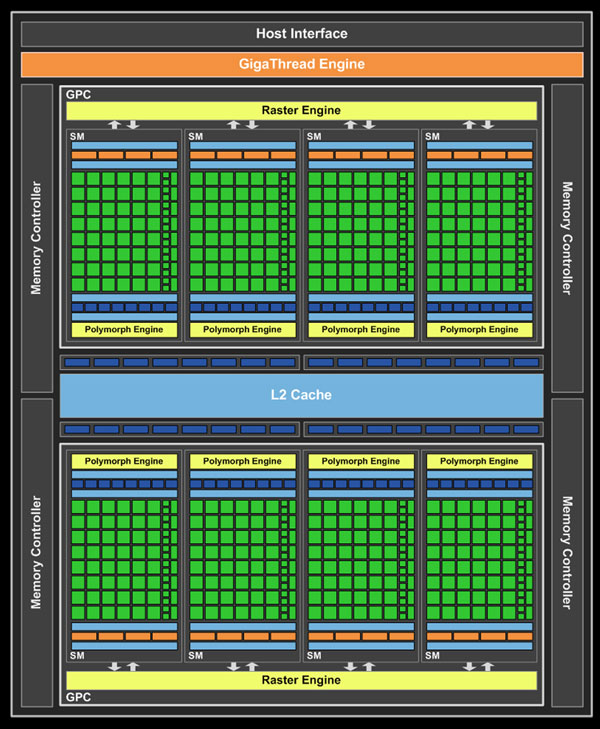
So how is NVIDIA accomplishing this? Much like what GF110 did for GF100, GF114 is doing for GF104. NVIDIA has resorted to tinkering with the Fermi family at a low level to optimize their designs against TSMC’s mature 40nm process, paying much closer attention to the types of transistors used in order to minimize leakage. As a result of the more mature manufacturing process and NVIDIA’s optimizations, they are now able to enable previously disabled functional units and raise clock speeds while keeping these revised GPUs in the same power envelopes as their first-generation predecessors. This is allowing NVIDIA to improve performance and/or power consumption even though these revised chips are virtually identical to their predecessors.
On GF110, we saw NVIDIA choose to take moderate gains in both performance and power consumption. In the case of GF114/GTX 560 however, NVIDIA is choosing to focus on improving performance while leaving power consumption largely unchanged – GTX 460 after all was a well-balanced part in the first place, so why change what already works?
In order to achieve the larger performance jump they’re shooting for, NVIDIA is tackling this from two sides. First of course is the enabling of previously disabled functional units – GTX 460 1GB had all 32 of its ROPs and associated hardware enabled, but only 7 of its 8 SMs enabled, leaving its geometry/shading/texturing power slightly crippled from what the GF104 chip was fully capable of. Like GF110/GTX 580, GF114/GTX 560 Ti will be a fully enabled part: all 384 CUDA Cores, 64 texture units, 8 Polymorph Engines, 32 ROPs, 512KB L2 cache, 4x64bit memory controllers are present, accounted for, and functional. Thus compared to GTX 460 1GB in particular, GTX 560 Ti immediately has more shading, texturing, and geometry performance than its predecessor, with roughly a 14% advantage over a similarly clocked GTX 460 1GB.
The other aspect of improving performance is improving the clockspeed. As you may recall GTX 460 was quite the charming overclocking card, as even without GPU overvolting we could routinely get 20% or more over the stock clock speed of 675MHz; to the point where NVIDIA tried to make an unofficial product out of partner cards with these lofty overclocks. For GTX 560 Ti NVIDIA has rolled these clocks in to the product, with GTX 560 Ti shipping at an 822MHz core clock and 1002MHz (4008MHz data rate) memory clock. This represents a 147Mhz (22%) core clock increase, and a more mild 102MHz (11%) memory clock increase over the GTX 460 1GB. Coupled with the aforementioned 14% increase in SMs, and it’s clear that there’s a quite a potential performance improvement for the GTX 560 even though we’re still technically looking at the same GPU.
As NVIDIA is not looking to significantly move the power envelope on the GTX 560 Ti compared to the GTX 460 1GB, the TDP remains similar. NVIDIA never specifies an idle TDP, but with their transistor level changes it should be lower. Meanwhile load TDP is going up by 10W, from 160W on the GTX 460 1GB to 170W on the GTX 560 Ti. 10W shouldn’t make for a significant difference, but it does drive home the point that NVIDIA is focusing more on performance at the slight expense of power this time around. GF114 is pin compatible with GF104, so partners can drop it in to existing GTX 460 designs, but those designs will need to be able to handle the extra power draw and heat. NVIDIA’s own reference design has been bulked up some, as we’ll see when we dissect the card.
The GTX 560 Ti will be launching at $249, roughly $20 higher than where the GTX 460 1GB started out but still targeted towards the same 1920x1200/1920x1080 resolution user base. Furthermore NVIDIA’s product stack will be shifting in response to the GTX 560 Ti. GTX 460 1GB is officially being moved down to make room for the GTX 560 Ti, and while NVIDIA isn’t providing MSRPs for it, the GTX 460 1GB can be found for as little as $150 after rebates right now – though this is largely a consequence of pricing wars with the AMD 6800 series rather than NVIDIA’s doing. Filling this nearly $100 gap for now will be factory overclocked GTX 460 1GBs. Meanwhile between the GTX 560 and GTX 570 will be a number of factory overclocked GTX 560s launching on day 1 (reusing GTX 460 designs). The GTX 470 is still on the market (and at prices below the GTX 560 for obvious reasons), but it’s not an official part of the stack and we expect supplies to dry up in due time.
NVIDIA’s marketing focus for the GTX 560 is to pair it with Intel’s recently launched Sandy Bridge CPUs, which have inspired a wave of computer upgrades that NVIDIA would like to hitch a ride with. Compared to the GTX 460 the GTX 560 isn’t a major upgrade on its own, and as a result NVIDIA is focusing more towards people upgrading their 8000/9000/GTX200 series equipped computers. Ultimately if you’re upgrading, NVIDIA would love to sell you a $250 GPU alongside a cheaper Core i5 2500K processor.
Meanwhile over at AMD they are shuffling their lineup and launching their own two-front counter-offensive. In terms of pricing and performance the GTX 560 Ti is between the Radeon HD 6950 and Radeon HD 6870, leaving AMD with a hole to fill. AMD has chosen to launch 1 new product – the Radeon HD 6950 1GB – to sit right above the GTX 560 Ti at $259, and in a move similar to how NVIDIA handled the Radeon HD 6800 series launch, push factory overclocked Radeon HD 6870s to go right below the GTX 560 Ti at around $230. The net result is that the price of reference-clocked 6870s has come down nearly $30 from launch, and can now be found for as little as $200. In any case, as there’s a great deal to discuss here, please see our companion article for the full-rundown on AMD’s GTX 560 Ti counter-offensive.
| Early 2011 Video Card MSRPs | ||
| NVIDIA | Price | AMD |
| $500 | ||
| $350 | Radeon HD 6970 | |
| $279-$299 | Radeon HD 6950 2GB | |
|
|
$259 | Radeon HD 6950 1GB |
|
GeForce GTX 560 Ti
|
$249 | |
| $219 | Radeon HD 6870 | |
| $160-170 | Radeon HD 6850 | |
The GF104/GF110 Refresher: Different Architecture & Different Transistors
For all practical purposes GF100 is the Fermi base design, but for sub high-end cards in particular NVIDIA has made a number of changes since we first saw the Fermi architecture a year and a half ago. For those of you reading this article who don’t regularly keep up with the latest NVIDIA hardware releases, we’re going to quickly recap what makes GF114 and GTX 560 Ti different from both the original GF100/GF110 Fermi architecture, and in turn what makes GF114 different from GF104 through NVIDIA’s transistor optimizations. If you’re already familiar with this, please feel free to skip ahead.
With that said, let’s start with architecture. The GF100/GF110 design is ultimately the compute and graphics monster that NVIDIA meant for Fermi to be. It has fantastic graphical performance, but it also extremely solid GPU computing performance in the right scenarios, which is why GF100/GF110 is the backbone of not just NVIDIA’s high-end video cards, but their Tesla line of GPU computing cards.
But Fermi’s compute characteristics only make complete sense at the high-end, as large institutions utilizing GPU computing have no need for weaker GPUs in their servers, and in the meantime home users don’t need features like ECC or full speed FP64 (at least not at this time) so much as they need a more reasonably priced graphics card. As a result only the high-end GF100/GF110 GPUs feature Fermi’s base design, meanwhile GF104 and later use a tweaked design that stripped away some aspects of Fermi’s GPU compute design while leaving much of the graphics hardware intact.
NVIDIA GF104 SM
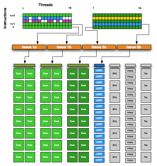
With GF104 we saw the first GPU released using NVIDIA’s streamlined Fermi architecture that forms the basis of GF104/GF106/GF108/GF114, and we saw a number of firsts from the company. Chief among these was the use of a superscalar architecture, the first time we’ve seen such a design in an NVIDIA part. Superscalar execution allows NVIDIA to take advantage of Instruction Level Parallelism (ILP) – executing the next instruction in a thread when it doesn’t rely on the previous instruction – something they haven’t done previously. It makes this streamlined design notably different from the GF100/GF110 design. And ultimately this design is more efficient than GF100/GF110 on average, while having a wider range of best and worst case scenarios than GF100/GF110, a tradeoff that doesn’t necessarily make sense for GPU computing purposes but does for mainstream graphics.
Meanwhile in terms of low-level design, starting with GF110 NVIDIA began revising the low-level design of their GPUs for production purposes. NVIDIA’s choice of transistors with GF10x was suboptimal, and as a result they used leaky transistors in functional units and parts thereof where they didn’t want them, limiting the number of functional units they could utilize and the overall performance they could achieve in the power envelopes they were targeting.
For GF110 NVIDIA focused on better matching the types of transistors they used with what a block needed, allowing them to reduce leakage on parts of the chip that didn’t require such fast & leaky transistors. This meant not only replacing fast leaky transistors with slower, less leaky transistors in parts of the chip that didn’t require such fast transistors, but also introducing a 3rd mid-grade transistor that could bridge the gap between fast/slow transistors. With 3 speed grades of transistors, NVIDIA was able to get away with only using the leakiest transistors where they needed to, and could conserve power elsewhere.
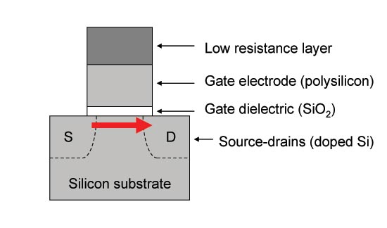
A typical CMOS transitor: Thin gate dielectrics lead to leakage
GF110 wasn’t the only chip to see this kind of optimization however, and the rest of the GF11x line is getting the same treatment. GF114 is in a particularly interesting position since as a smaller GPU, its predecessor GF104 wasn’t as badly affected. Though we can’t speak with respect to enabling additional functional units, at the clockspeeds and voltages NVIDIA was targeting we did not have any issues with the stock voltage. In short while GF100 suffered notably from leakage, GF104 either didn’t suffer from it or did a good job of hiding it. For this reason GF114 doesn’t necessarily stand to gain the same benefit.
As we touched on in our introduction, NVIDIA is putting their gains here in to performance rather than power consumption. The official TDP is going up 10W, while performance is going up anywhere between 10% and 40%. This is the only difference compared to GF104, as GF114 does not contain any architectural changes (GF110’s changes were backported from GF104). Everything we see today will be a result of a better built chip.
Meet The GTX 560 Ti
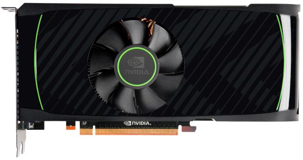
As we mentioned previously, GF114 is so similar to GF104 that it’s even pin compatible, leading to a number of NVIDIA’s partners simply reusing their GTX 460 designs. So long as you can provide the extra 10W and handle the extra heat, a GTX 460 design is 1 GF114 away from being a GTX 560 Ti. And while we’re going to see a number of familiar designs from NVIDIA’s partners, that hasn’t stopped NVIDIA from going back to the drawing table for the GTX 560 Ti’s reference design. As a result while the reference card is similar to the GTX 460 reference card, it has also clearly been enhanced to not just handle the slightly higher power requirements but to go above and beyond.
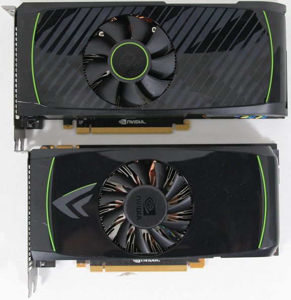
Top: GTX 560 Ti. Bottom: GTX 460 1GB
Since so much of this article is based on comparisons to the GTX 460, let’s start there. GTX 460 was an 8.25” long card with a center-mounted fan using a half-enclosed shroud, sitting on top of a slightly odd dual-heatpipe heatsink. By using a center-mounted fan, NVIDIA went with a design that recirculates some air in the case of the computer instead of a blower that fully exhausts all hot air. The advantage of the recirculating design is that it’s quieter than a blower, but the cost is that it’s more reliant on case ventilation. In a well-ventilated case like our Thermaltake Spedo, this worked out well to the GTX 460’s advantage, resulting in a very cool, very quiet card. In fact the only real problem we encountered with NVIDIA’s design was on the similarly designed GTS 450, where were discovered the downside to the fact that the PCB wasn’t securely mounted to the shroud on all corners.
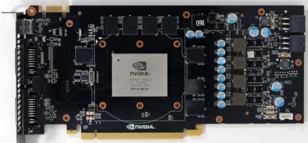
For the GTX 560 Ti, NVIDIA has taken this same basic design and has effectively built it bigger. Overall the GTX 560 Ti is now bigger, measuring a full 9” long. This looks to be a result of both a larger heatsink, and of additional components laid out on the PCB (presumably to meet the higher power requirements). Anchoring that 9” PCB is a baseplate, nearly identical in style to the one we see on the GTX 580 and GTX 570. As a simple metal plate the baseplate provides some heatsink capacity for any small components it sits over (e.g. MOSFETs) but it also provides mount points for OEM computers that further bolt down their video cards, and it provides structural stability to the now longer card; the GTX 560 Ti won’t bend, and trust me I’ve tried.
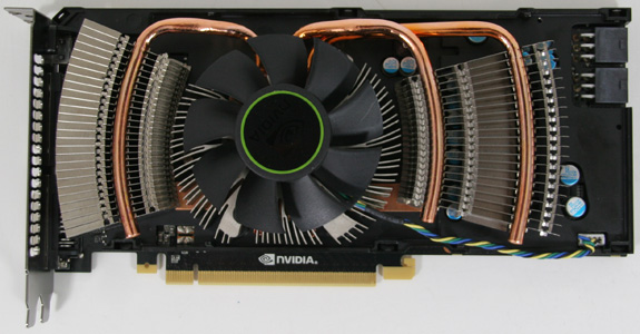
Cooling is being provided by a heatsink & fan combination similar to the GTX 460. Like everything else about the card this has been scaled up a bit to meet the higher power requirements, with a slightly longer heatsink attached to the GPU using 3 copper heatpipes. Sitting over this is an equally similar partially open shroud which directs air out the front and the rear of the card. For lack of better wording the shroud is slightly more enclosed on the GTX 560 Ti than the GTX 460, so we suspect at least a trivial amount of additional hot air gets exhausted towards the front of the card outside of the case, as opposed to on the GTX 460. Finally the shorud is once more concave, resulting in the 80mm fan sticking up above the shroud slightly for better airflow.
Looking at the bare PCB, as was the case with the GF104 GPU, GF114 is capped with a metal heatspreader. Meanwhile the memory on our sample is 5Gbps Samsung GDDR5, which is rated well beyond the 4004MHz the card ships as. As we’ve mentioned before the limitation becomes the memory controller and the memory bus, long before it becomes the GDDR5 memory itself. Providing power for all of this is a pair of 6pin PCIe power sockets, which are located on the rear of the card. We’re not fans of rear mounted plugs, particularly on longer cards. We would have liked to see NVIDIA rotate them upwards given the GTX 560 Ti’s extended length.
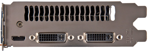
Meanwhile display connectivity remains unchanged from the rest of the GTX 400/500 series. NVIDIA provides 2 dual-link DVI ports and a mini-HDMI port; however only 2 displays can be driven by a single card. Through SLI a second card can be hooked up to drive a 3rd and 4th display, necessary among other things for NVIDIA/3D Vision Surround. As with the GTX 460, a single SLI connector is provided, allowing 2-way SLI.
Overall while the GTX 560 Ti isn’t necessarily overbuilt, it’s certainly more than we were expecting for just a 10W increase in power consumption. Whether NVIDIA actually needed a card like this or if they have a specific goal in mind we’re unsure, but it’s quite a bit more complex a card than the GTX 460. No doubt this drives part of the GTX 560 Ti’s higher price, but given that NVIDIA’s partners can sell GTX 460 1GBs for nearly $100 less, there’s probably a good profit to be had with this card even with its additional complexity. Or to put things another way, even with the additional complexity we suspect NVIDIA has plenty of room to lower prices as the competitive market dictates.
If you’ve made it this far then no doubt the name has caught your attention. NVIDIA’s product naming has been complex (if not exploitive) lately, and GTX 560 Ti doesn’t change that. Unlike GF100 to GF110, GF104 to GF114 brings with it absolutely no architectural changes whatsoever. Thus GTX 560 is nothing more than a GTX 460 with more functional units and a higher clockspeed based on a tweaked chip ; hardly deserving of a whole new generation in name. But we knew this was coming the moment we saw the GTX 580, so here we are.
Furthermore NVIDIA’s affinity for long names continues to grow at roughly the same pace as the length of their product names. Due to NVIDIA’s disabling of ROPs on the GTX 460 the memory size was an unofficial suffix, as cards with 768MB would have fewer ROPs and less memory bandwidth, leading to performance even lower than what the missing 256MB on its own would lead to. The good news is that NVIDIA has improved on this by ditching the memory suffixes (memory size is no longer used to indicate the number of ROPs), while the bad news is that suffixes are here to stay.
While NVIDIA had used suffixes for a long time, starting with the 200 series however suffixes became the prefix, leading to GTX 285, GTS 250, GT 430, etc. After a two and a half year break from suffixes, they’re back. In a rather transparent attempt to capture the goodwill and fame of the company’s GeForce 3 Ti and GeForce 4 Ti products, NVIDIA is resurrecting the Ti suffix for the GTX 560 Ti. At this point in time it doesn’t mean anything, but if the GTX 460 is anything to go by, at some point we’d expect to see a lower-end GeForce GTX 560 <insert suffix here> to flesh out NVIDIA’s lineup. It goes without saying that we’d rather just have model numbers that clearly denote the performance ranking of cards, e.g. GTX 560, GTX 555, etc, but then we’re hardware enthusiasts and not marketing directors.
The Test
Launching virtually alongside the GTX 560 Ti is NVIDIA’s latest driver branch, Forceware Release 265, with the first WHQL driver being 266.58. Released in beta form earlier this month and in its WHQL form last week, 265 contains the usual mix of documented performance increases (particularly with SLI), bug fixes, and ancillary improvements such as supporting 3D Vision in windowed mode. Most important to our testing are the optimizations that NVIDIA made to their drivers for Civilization V, and their OpenCL drivers; scores in both those areas have gone way up. Elsewhere performance is largely consistent for single card setups, while SLI gains are a bit more consistent.
Please note that for the time being we’re focusing on single card performance, as we have not had the time to update all of our SLI configurations to take in to account these new drivers. We’ll be looking at GTX 560 Ti SLI performance a bit later this week once we’ve revised all of our SLI results.
For our 400 and 500 series cards we’re using the newly released 266.58 drivers, while for the GTX 560 Ti we’re using the beta 266.56 drivers – which as near as we can tell are identical save for the fact that 266.58 didn’t build in GTX 560 Ti support. Meanwhile the GTX 200 series and below continues to use 262.99.
On the AMD side of things we’re adding the newly launched Radeon HD 6950 1GB. Most of the time performance is identical to the 2GB version, but as we’ve seen in our 6950 1GB companion launch article, there is a difference at times.
Finally, for NVIDIA cards all tests were done with default driver settings unless otherwise noted. As for AMD cards, we are disabling their new AMD Optimized tessellation setting in favor of using application settings (note that this doesn’t actually have a performance impact at this time), everything else is default unless otherwise noted.
| CPU: | Intel Core i7-920 @ 3.33GHz |
| Motherboard: | Asus Rampage II Extreme |
| Chipset Drivers: | Intel 9.1.1.1015 (Intel) |
| Hard Disk: | OCZ Summit (120GB) |
| Memory: | Patriot Viper DDR3-1333 3 x 2GB (7-7-7-20) |
| Video Cards: |
AMD Radeon HD 6970 AMD Radeon HD 6950 2GB AMD Radeon HD 6950 1GB AMD Radeon HD 6870 AMD Radeon HD 6850 AMD Radeon HD 5970 AMD Radeon HD 5870 AMD Radeon HD 5850 AMD Radeon HD 5770 AMD Radeon HD 4870 NVIDIA GeForce GTX 580 NVIDIA GeForce GTX 570 NVIDIA GeForce GTX 560 Ti NVIDIA GeForce GTX 480 NVIDIA GeForce GTX 470 NVIDIA GeForce GTX 460 1GB NVIDIA GeForce GTX 460 768MB NVIDIA GeForce GTS 450 NVIDIA GeForce GTX 285 NVIDIA GeForce GTX 260 Core 216 |
| Video Drivers: |
NVIDIA ForceWare 262.99 NVIDIA ForceWare 266.56 Beta NVIDIA ForceWare 266.58 AMD Catalyst 10.10e AMD Catalyst 11.1a Hotfix |
| OS: | Windows 7 Ultimate 64-bit |
Crysis: Warhead
Kicking things off as always is Crysis: Warhead, still one of the toughest game in our benchmark suite. Even 2 years since the release of the original Crysis, “but can it run Crysis?” is still an important question, and the answer continues to be “no.” While we’re closer than ever, full Enthusiast settings at a playable framerate is still beyond the grasp of a single card.
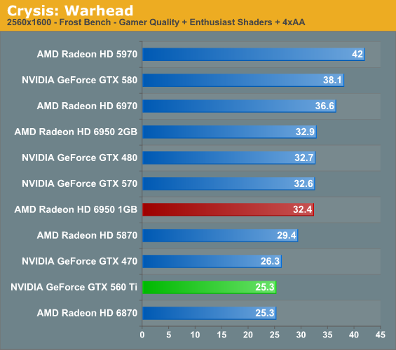
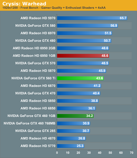
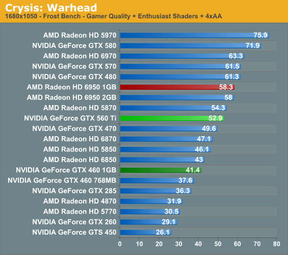
While we throw in our 2560x1600 charts for good measure, the real chart to keep an eye on is at 1920x1200, the kind of resolution cards around this price range are targeted at. With that in mind, our first game – and often a prognostic of overall performance – is not in NVIDIA’s favor. The 6950 does quite well here, leaving the GTX 560 down by well more than the 4% price difference between the cards. Overall we’re looking at performance fairly close to the older 5870 in Crysis.
Amidst NVIDIA’s own stable of products, what becomes clear is that the GTX 560 has a close peer in the soon to be phased out GTX 470. At 1920 and 1680 the GTX 560 is always faster than the GTX 470, but never immensely so; and at higher resolutions the GTX 470 still has an advantage. Meanwhile the GTX 460 1GB is outclassed by a consistent 28%. It’s not bad for what’s technically the same GPU, eh?
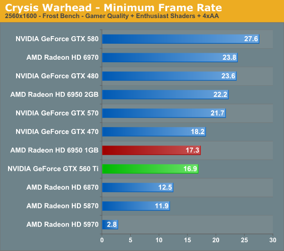
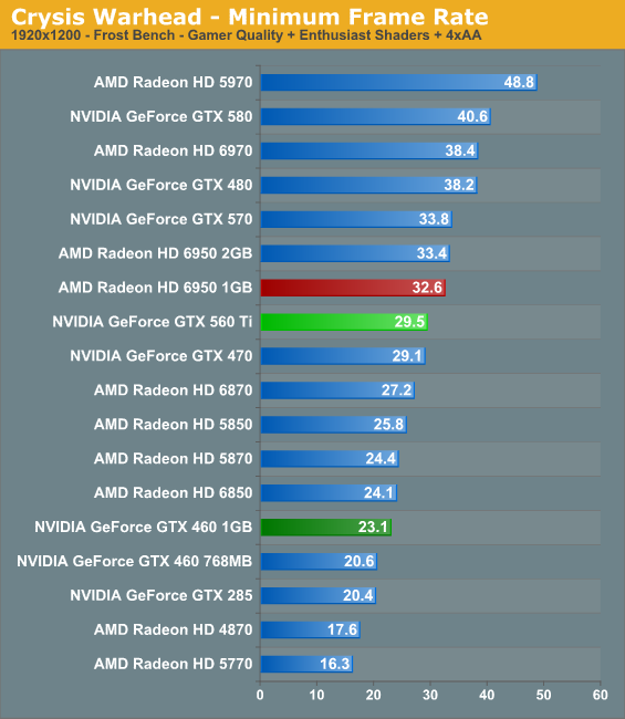
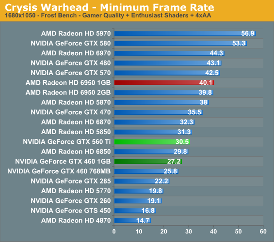
The story of minimums is even a bit more lopsided against NVIDIA here. The lower the resolution the more it falls behind the 6950 1GB, by 15% at 1920 and 25% at 1680. However on a positive note, on an absolute basis the 560 is doing pretty well here; at 29.5fps minimum at 1920, it’s basically never falling below 30fps, meaning not only can it play Crysis but that it can do so smoothly. It is quite interesting to note though that the 560’s minimums are almost identical at 1920 and 1680, indicating a non-resolution dependent bottleneck. ROPs and/or memory bandwidth look to be the culprit here, particularly with the GTX 460 1GB coming so close at 1680.
BattleForge
Up next is BattleForge, Electronic Arts’ free to play online RTS. As far as RTSes go this game can be quite demanding, and this is without the game’s DX11 features.
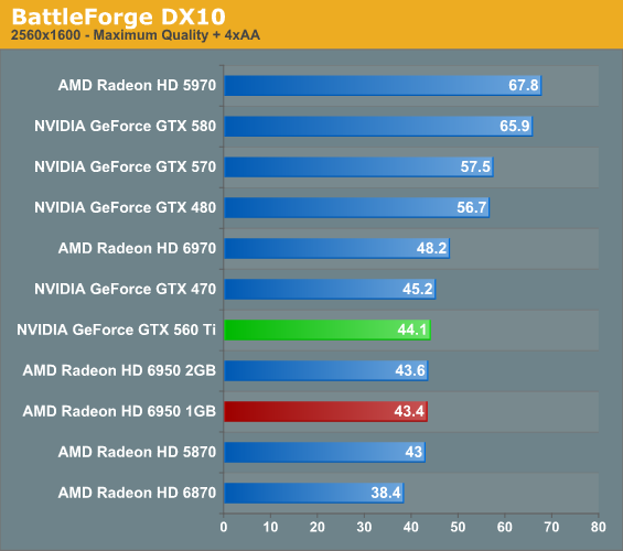
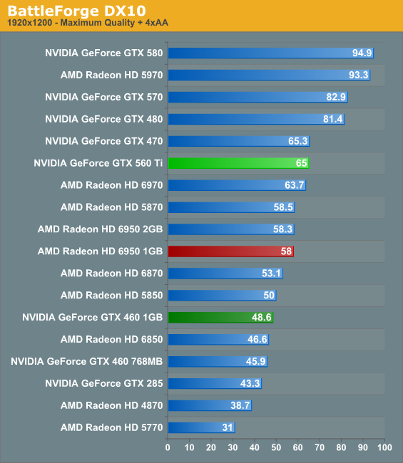
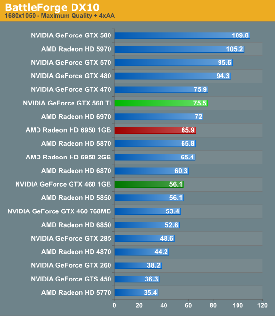
With BattleForge we see the beginning of the same win-some/lose-some results that we saw with the Radeon HD 6900 series versus the GTX 500 series. For as well as the 6900 series did at Crysis, the tables are turned here with BattleForge with the GTX 560 taking a 10-15% lead over the 6950 1GB; even the 6970 itself here falls by at least a frame or two per second. Traditionally NVIDIA does very well in this game, and here it shows to the GTX 560’s benefit.
Meanwhile compared to the GTX 470 we’re looking at a dead heat, and against the GTX 460 1GB the advantage is now to 33% in the GTX 560’s favor.
Metro 2033
The next game on our list is 4A Games’ Metro 2033, their tunnel shooter released last year. In September the game finally received a major patch resolving some outstanding image quality issues with the game, finally making it suitable for use in our benchmark suite. At the same time a dedicated benchmark mode was added to the game, giving us the ability to reliably benchmark much more stressful situations than we could with FRAPS. If Crysis is a tropical GPU killer, then Metro would be its underground counterpart.
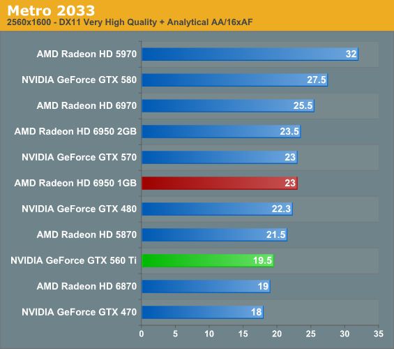
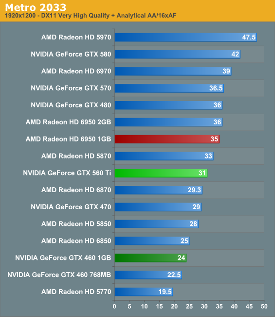
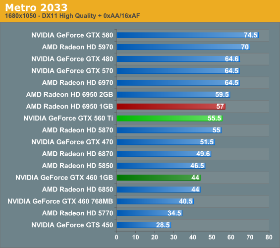
Another game, another flip-flop. Here we see the GTX 560 come in under the 6950 1GB by around 10% at 1920, and closing the gap at 1680 where we don’t use as many advanced features. It’s quite a situation to be seeing the performance of the GTX 560 flip between near-6870 performance and near-6970 performance, and at the same time cementing the fact that the best GPU for any given game is highly, highly dependent on the game.
Meanwhile at 1920 though the GTX 560 does gather the distinction of being the bare minimum GeForce card needed to get Metro to or above a 30fps average, showcasing just how stressful the game is.
HAWX
Ubisoft’s 2008 aerial action game is one of the less demanding games in our benchmark suite, particularly for the latest generation of cards. However it’s fairly unique in that it’s one of the few flying games of any kind that comes with a proper benchmark.
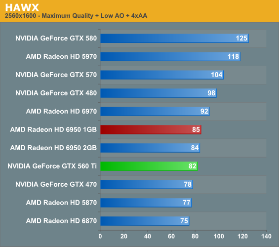
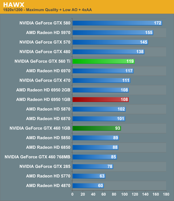
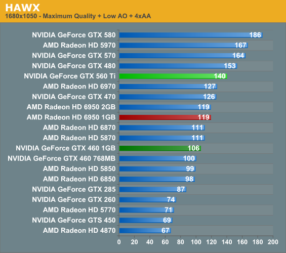
Under HAWX the GTX 560 is once more ahead of our pack, edging out the 6970 and beating the 6950 1GB by 10% at 1920 and 17% at 1680. At 2560 we do see the 560 finally fall behind the 6950, but at the same time we’re looking at a situation where even the slowest card in that chart is well above 60fps.
HAWX is not normally a game we consider shader limited, so compared to NVIDIA’s other cards the results are particularly interesting. The GTX 470 is still hanging on for dear life, but the lower the resolution the wider the gap becomes. Meanwhile over the GTX 460 1GB the lead is still 30% even though we haven’t changed the ROP count, showcasing that there’s more ROP clocks involved in the 560’s advantage over the 460.
Civilization V
The other new game in our benchmark suite is Civilization 5, the latest incarnation in Firaxis Games’ series of turn-based strategy games. Civ 5 gives us an interesting look at things that not even RTSes can match, with a much weaker focus on shading in the game world, and a much greater focus on creating the geometry needed to bring such a world to life. In doing so it uses a slew of DirectX 11 technologies, including tessellation for said geometry and compute shaders for on-the-fly texture decompression.
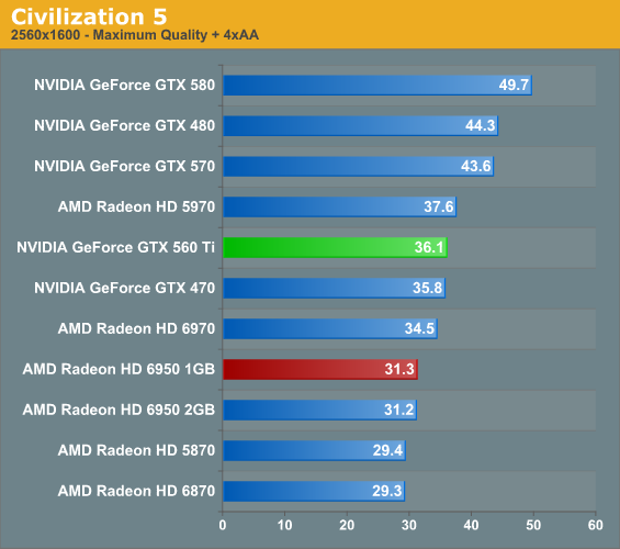
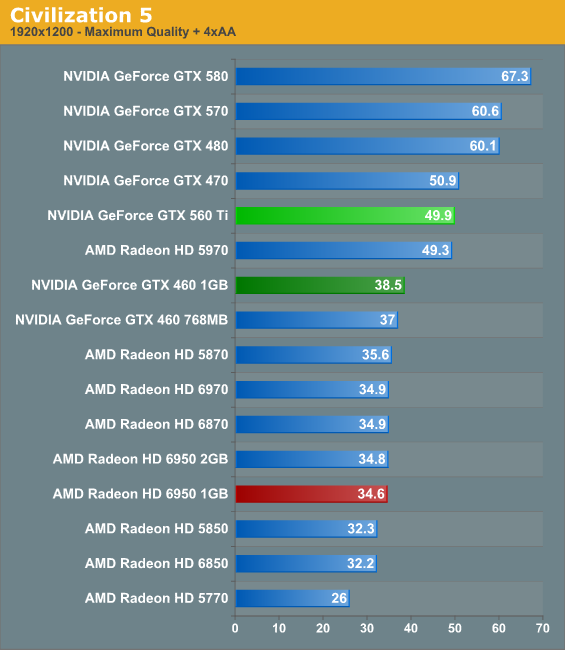
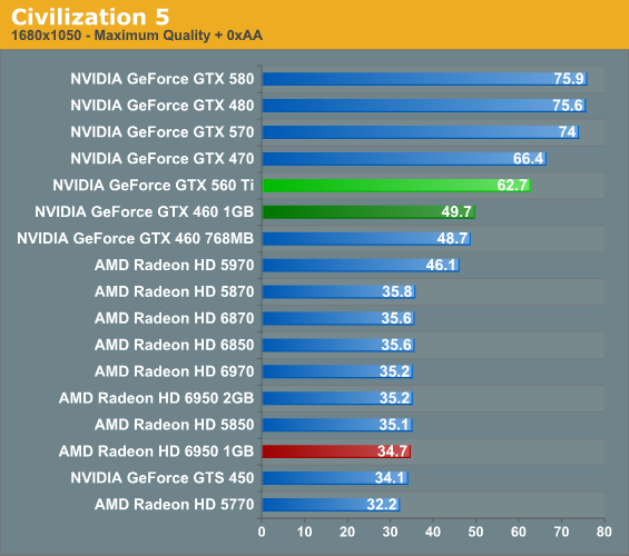
We have always considered Civ 5 an interesting game both for its near-complete use of the DX11 feature set, and because of its interesting performance characteristics. 2 weeks ago we called it CPU limited based on the fact that once we had sufficiently powerful cards, AMD and NVIDIA results tended to clump together despite any difference in their respective cards’ speed. With the Forceware Release 265 drivers, NVIDIA has blown this assumption apart, with NVIDIA’s more powerful cards launching ahead at 1920 and lower. We appear to be quite GPU limited on the NVIDIA side all of a sudden, which is about as drastic change as we could expect. Furthermore NVIDIA is holding their cards close to their chest on this – they’ve obviously found a wonder optimization, but they aren’t ready to say what it is.
In any case while AMD has always trailed NVIDIA in single card performance in Civ 5, with these driver changes it’s quite monumental. The GTX 560 Ti is 44% faster than the 6950 at 1920, 80% faster at 1680, and even the GTX 460 768MB can edge out the 6970 at 1920. Whatever NVIDIA has done, it has made Civilization V quite a lot faster and smoother at 1920 and 1680, particularly when a large number of units are on screen.
Among NVIDIA’s own cards the lead has actually shrunk some compared to our earlier games. The GTX 470 has an edge on the GTX 560, and the 560 in turn is down to a 25%-30% lead over the GTX 460 1GB. We don’t seem to be ROP or memory bandwidth limited, so perhaps this is a case of the GF104/GF114 architecture’s shaders underperforming?
Battlefield: Bad Company 2
The latest game in the Battlefield series - Bad Company 2 – remains as one of the cornerstone DX11 games in our benchmark suite. As BC2 doesn’t have a built-in benchmark or recording mode, here we take a FRAPS run of the jeep chase in the first act, which as an on-rails portion of the game provides very consistent results and a spectacle of explosions, trees, and more.
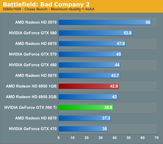
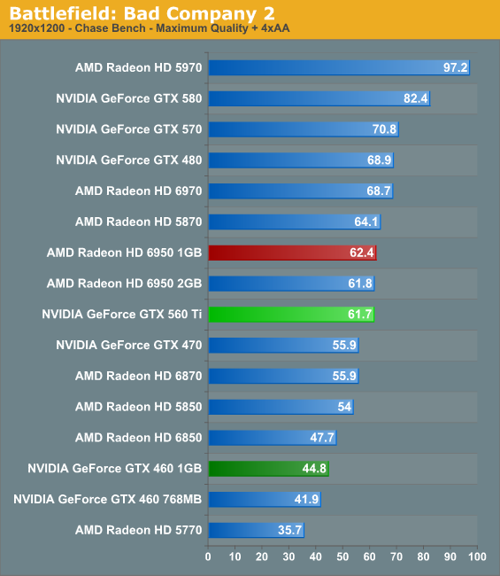
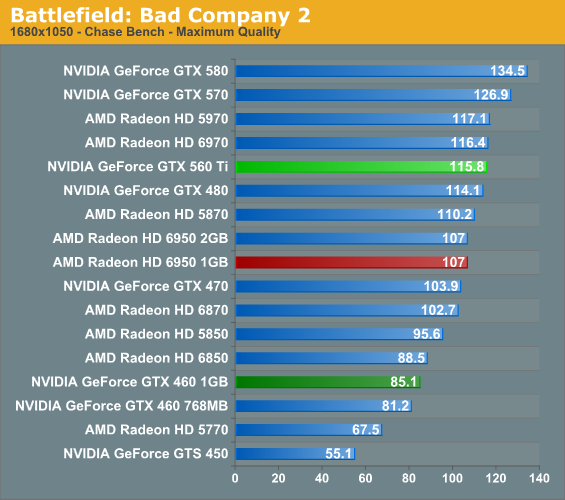
Even more so than HAWX, Bad Company 2 marks the closest we’ve seen the GTX 560 and the 6950 1GB. At 1920 the 6950 has a lead of under a frame per second, and it’s not until 1680 that we see the GTX 560 take any kind of lead. In this case both cards just pass the all-important 60fps mark at 1920, representing the bottom necessary for (more or less) fully fluid gameplay.
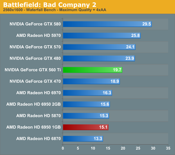
While we’re not generally interested in 2560 with the GTX 560, it is the only resolution that we run our Waterfall benchmark on, so we’ll quickly comment. NVIDIA normally does quite well here and the GTX 560 is no exception – even though it loses at this resolution on average, it’s 30% faster when it comes to minimums. We’ve seen the minimums in Crysis go the other way, so minimums seem just as game-dependent as the averages with all things considered.
STALKER: Call of Pripyat
The third game in the STALKER series continues to build on GSC Game World’s X-Ray Engine by adding DX11 support, tessellation, and more. This also makes it another one of the highly demanding games in our benchmark suite.
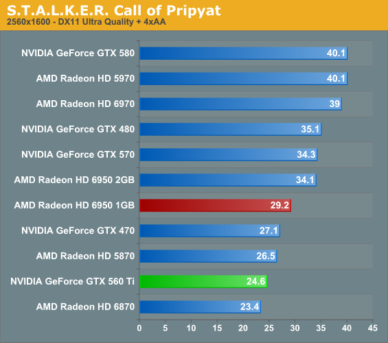
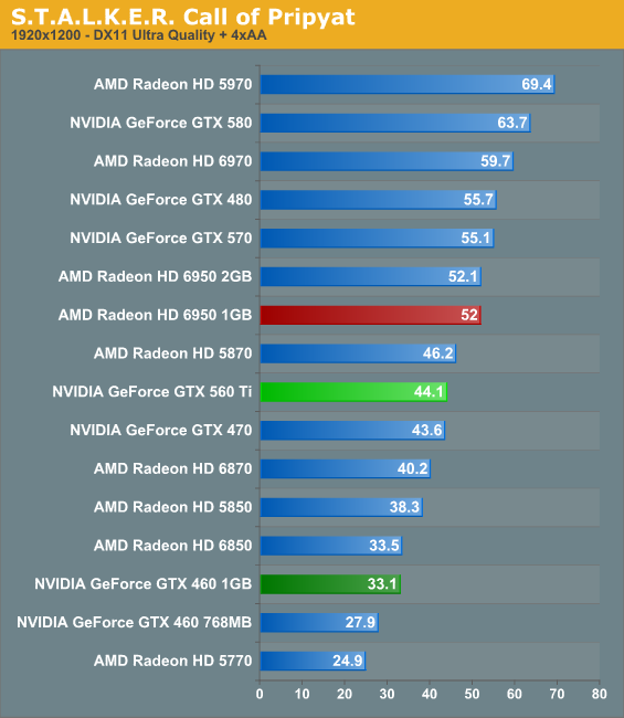
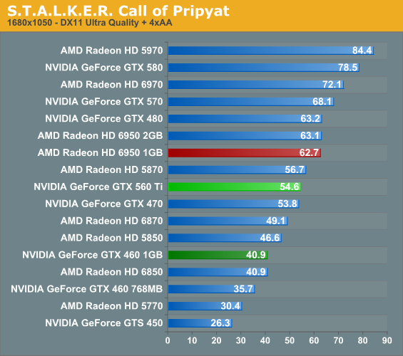
With STALKER being another game that normally favors AMD, there’s no surprise here that the GTX 560 comes up short. The GTX 560 underperforms AMD’s latest by 10%-15% depending on the resolution. The GTX 560’s advantage over the GTX 460 1GB is still a very healthy 33% however, so it certainly looks like we’re seeing the differences in shader architectures in action.
DIRT 2
Codemasters’ 2009 off-road racing game continues its reign as the token racer in our benchmark suite. As the first DX11 racer, DiRT 2 makes pretty thorough use of the DX11’s tessellation abilities, not to mention still being the best looking racer we have ever seen.
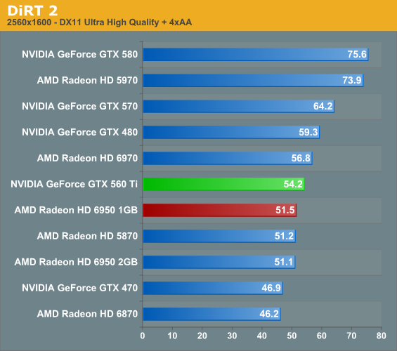
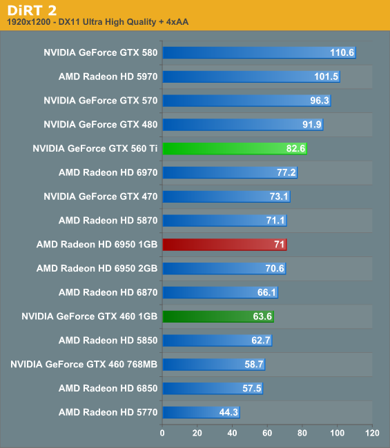
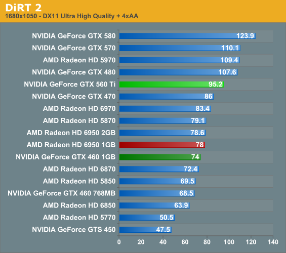
We’re once more looking at a game that generally favors NVIDIA cards, so there are not a lot of surprises to find in our results. The GTX 560 enjoys a 15% lead over the 6950 1GB at 1920, and it even enjoys a small lead over the 6970. As far as NVIDIA’s cards are concerned we’re looking at a typical 30% advantage over the GTX 460 1GB, and interestingly enough even the GTX 470 is nearly 10fps behind at 1920 resolution.
Mass Effect 2
Electronic Arts’ space-faring RPG is our Unreal Engine 3 game. While it doesn’t have a built in benchmark, it does let us force anti-aliasing through driver control panels, giving us a better idea of UE3’s performance at higher quality settings. Since we can’t use a recording/benchmark in ME2, we use FRAPS to record a short run.
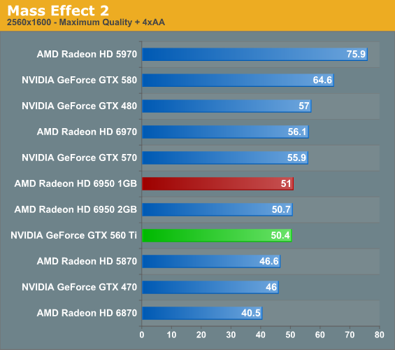
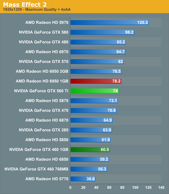
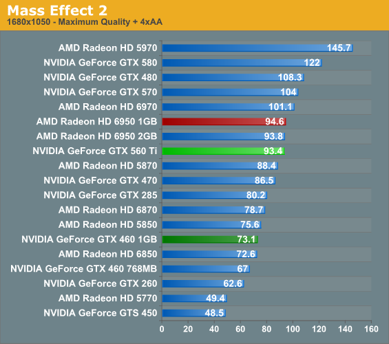
Finally we once again have a close race to look at with Mass Effect 2. The 6950 1GB does enjoy a 7% lead at 1920, while this lead largely evaporates at 1680. The 5870 comparison once again seems appropriate though, as at the same resolution the GTX 560 is practically tied. Meanwhile at the same resolution we’re looking at one of the smaller leads the GTX 560 enjoys over the GTX 460 1GB, bagging only a 23% lead – roughly in line with the clockspeed increase. This makes it likely that we’re ROP limited, at least at this resolution.
Wolfenstein
Finally among our benchmark suite we have Wolfenstein, the most recent game to be released using the id Software Tech 4 engine. All things considered it’s not a very graphically intensive game, but at this point it’s the most recent OpenGL title available. It’s more than likely the entire OpenGL landscape will be thrown upside-down once id releases Rage later this year.
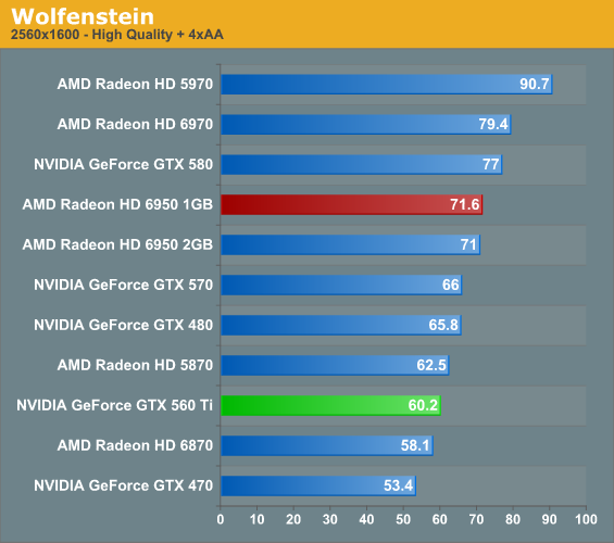
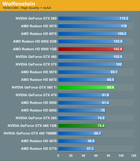
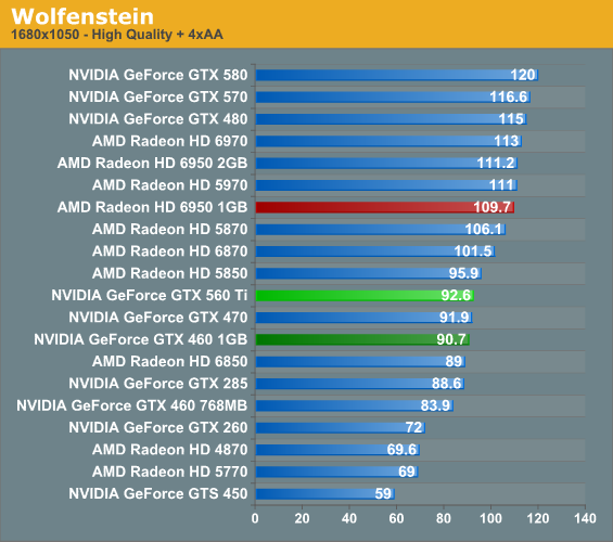
Wolfenstein is quite easy to make CPU limited even at higher resolutions, so the range on our charts is compressed some here. Even against the risk of being CPU limited, the 6950 1GB has a solid lead over the GTX 560 here at both 1920 and 1680, showcasing either an NVIDIA weakness at Wolfenstein, or possibly a larger weakness at OpenGL as a whole. Among the NVIDIA cards the GTX 560’s lead over the GTX 460 1GB is the lowest we’ve ever seen it: 20% at 1920, and all of 2% at a 1680. NVIDIA is definitely CPU limited here, if not also memory bandwidth limited.
Compute & Tessellation
Moving on from our look at gaming performance, we have our customary look at compute performance, bundled with a look at theoretical tessellation performance. Unlike our gaming benchmarks where NVIDIA’s architectural differences between GF114 and GF110 are largely irrelevant, they can become much more important under a compute-bound situation depending on just how much ILP can be extracted for the GTX 560 Ti.
Our first compute benchmark comes from Civilization V, which uses DirectCompute to decompress textures on the fly. Civ V includes a sub-benchmark that exclusively tests the speed of their texture decompression algorithm by repeatedly decompressing the textures required for one of the game’s leader scenes.
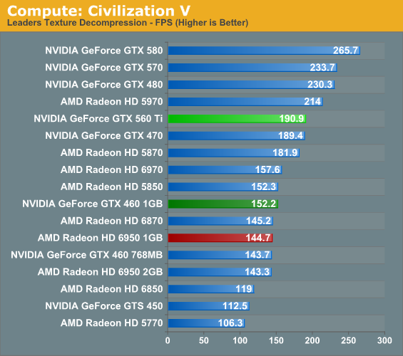
Under our Civilization 5 compute benchmark we have a couple of different things going on even when we just look at the NVIDIA cards. Compared to the GTX 460 1GB, the GTX 560 enjoys a 31% performance advantage; this is less than the theoretical maximum of 39%, but not far off from the performance advantages we’ve seen in most games. Meanwhile the GTX 470 is practically tied with the GTX 560 even though on paper the GTX 560 has around a 15% theoretical performance advantage. This ends up being a solid case of where the limitations of ILP come in to play, as clearly the GTX 560 isn’t maximizing the use of its superscalar shaders. Or to put it another way, it’s an example as to why NVIDIA isn’t using a superscalar design on their Tesla products.
Meanwhile this benchmark has always favored NVIDIA’s architectures, so in comparison to AMD’s cards there’s little to be surprised about. The GTX 560 Ti is well in the lead, with the only AMD card it can’t pass being the dual-GPU 5970.
Our second GPU compute benchmark is SmallLuxGPU, the GPU ray tracing branch of the open source LuxRender renderer. While it’s still in beta, SmallLuxGPU recently hit a milestone by implementing a complete ray tracing engine in OpenCL, allowing them to fully offload the process to the GPU. It’s this ray tracing engine we’re testing.
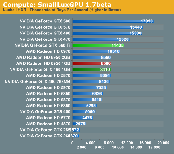
Small Lux GPU is the other test in our suite where NVIDIA’s drivers significantly revised our numbers. Where this test previously favored raw theoretical performance, giving the vector-based Radeons an advantage, NVIDIA has now shot well ahead. Given the rough state of both AMD and NVIDIA’s OpenCL drivers, we’re attributing this to bug fixes or possibly enhancements in NVIDIA’s OpenCL driver, with the former seeming particularly likely. However NVIDIA is not alone when it comes to driver fixes, and AMD has seem a similar uptick against the newly released 6900 series. It’s not nearly the leap NVIDIA saw, but it’s good for around 25%-30% more rays/second under SLG. This appears to be accountable to further refinement of AMD’s VLIW4 shader compiler, which as we have previously mentioned stands to gain a good deal of performance as AMD works on optimizing it.
So where does SLG stack up after the latest driver enhancements? With NVIDIA’s rocket to the top, they’re now easily dominating this benchmark. The GTX 560 Ti is now slightly ahead of the 6970, never mind the 6950 1GB where it has a 33% lead. Rather than being a benchmark that showed the advantage of having lots of theoretical compute performance, this is now a benchmark that seems to favor NVIDIA’s compute-inspired architecture.
Our final compute benchmark is a Folding @ Home benchmark. Given NVIDIA’s focus on compute for Fermi, cards such as the GTX 560 Ti can be particularly interesting for distributed computing enthusiasts, who are usually looking for a compute card first and a gaming card second.
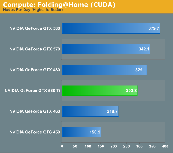
Against the senior members of the GTX 500 series and even the GTX 480 the GTX 560 Ti is still well behind, but at the same time Folding @ Home does not look like it significantly penalizes GTX 560’s superscalar architecture.
At the other end of the spectrum from GPU computing performance is GPU tessellation performance, used exclusively for graphical purposes. With Fermi NVIDIA bet heavily on tessellation, and as a result they do very well at very high tessellation factors. With 2 GPCs the GTX 560 Ti can retire 2 triangles/clock, the same rate as the Radeon HD 6900 series, so this should be a good opportunity to look at theoretical architectural performance versus actual performance.
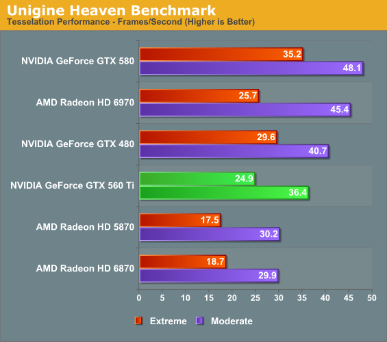
Against the AMD 5800 and 6800 series, the GTX 560 enjoys a solid advantage, as it’s able to retire twice as many triangles per clock as either architecture. And while it falls to both GTX 480 and GTX 580, the otherwise faster Radeon HD 6970 is close at times – at moderate tessellation it has quite the lead, but the two are neck-and-neck at extreme tessellation where triangle throughput and the ability to efficiently handle high tessellation factors counts for everything. Though since Heaven is a synthetic benchmark at the moment (the DX11 engine isn’t currently used in any games) we’re less concerned with performance relative to AMD’s cards and more concerned with performance relative to the other NVIDIA cards.
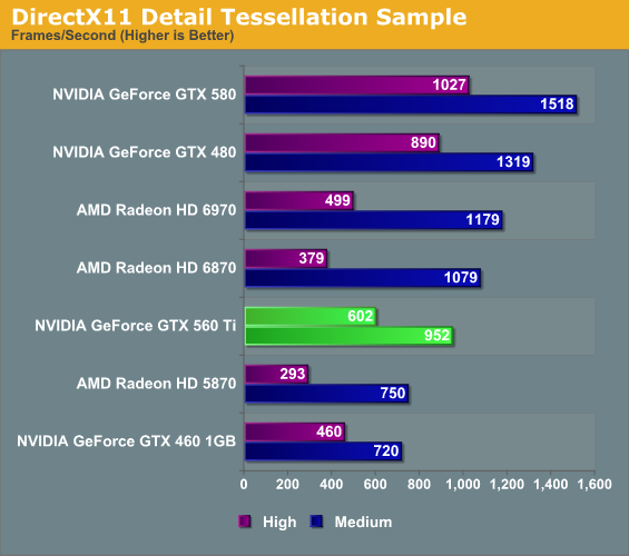
Microsoft’s Detail Tessellation sample program showcases NVIDIA’s bet on tessellation performance even more clearly. NVIDIA needs very high tessellation factors to shine compared to AMD’s cards. Meanwhile against the GTX 460 1GB our gains are a bit more muted; even though this is almost strictly a theoretical test, the GTX 560 only gains 30% on the GTX 460. Ultimately while the additional SM unlocks another tessellator on NVIDIA’s hardware, it does not unlock a higher triangle throughput rate, which is dictated by the GPCs.
Power, Temperature, & Noise
Last but not least as always is our look at the power consumption, temperatures, and acoustics of the GTX 570. While NVIDIA chose to optimize for both performance and power on the GTX 570/580, the GTX 560 Ti is almost exclusively optimized for performance. As a result NVIDIA’s official TDP has gone up by 10W, and as we’ll see in practice the difference is even greater than that.
| GeForce 400/500 Series Load Voltage | ||||
| Ref GTX 560 Ti | Ref GTX 460 1GB | Ref GTX 460 768MB | ||
| 0.950v | 1.025v | 0.987v | ||
Starting with VIDs, we once again only have 1 card so there’s not too much data we can draw. Our GTX 560 sample has a VID of 0.95v, which is actually lower than our reference 1GB card, which had a VID of 1.025v. NVIDIA’s transistor optimizations can allow them to run their cards at lower voltages compared to the earlier designs, but at the same time based on our data a lower VID appears to be critical for keeping the GTX 560 Ti’s power consumption from significantly growing versus the GTX 460. This is not wholly unexpected – GF104 never suffered from leakage nearly as badly as GF100 did.
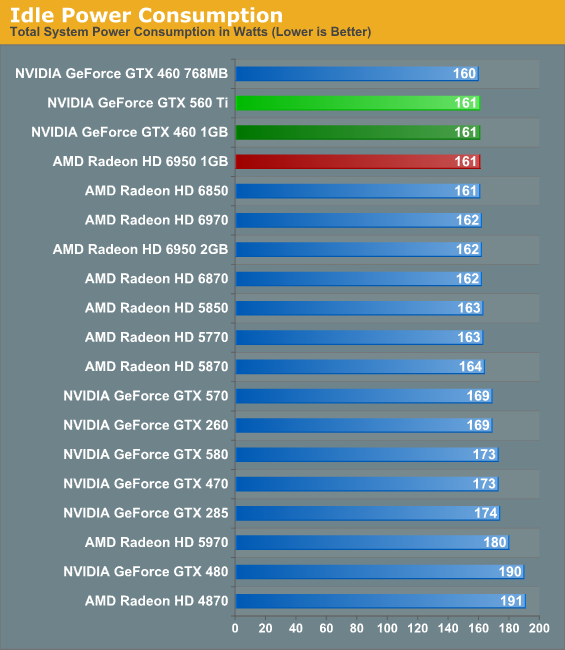
Idle power is effectively a wash here. The GTX 560 Ti does have additional functional units which are now consuming power even when the GPU is idling, but at the same time the transistor changes are keeping idle power in check. At 161W it’s as good as the rest of our mid-range cards.
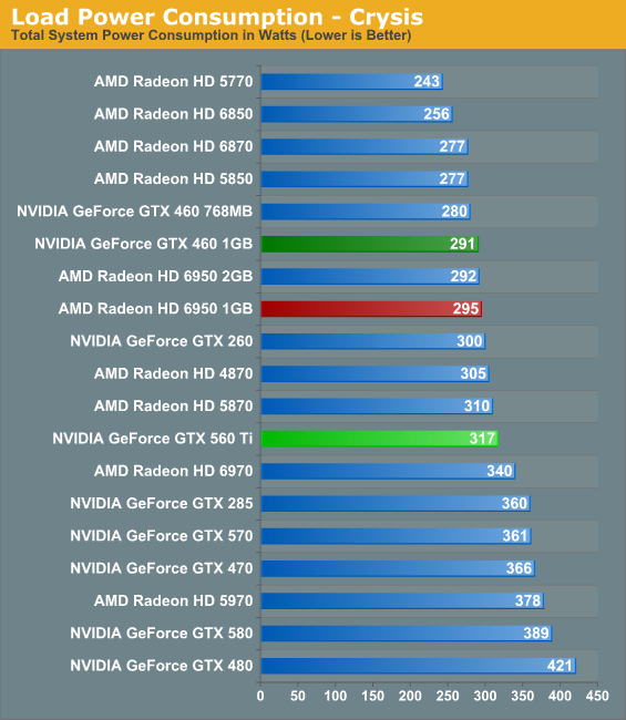
Under Crysis we get our first glimpse that while NVIDIA’s TDP may only be 10W higher, the real world difference is greater. While we cannot isolate just the power consumption of the video card, and we can explain at least some of the difference as being a result of a greater workload on the CPU due to a higher framerate, we can’t fully explain away the difference between the GTX 460 1GB and the GTX 560 Ti. With a 26W delta, we’re confident the extra power draw we’re seeing with the GTX 560 Ti is well over 10W – and keep in mind this is a game test where our numbers are similar to how NVIDIA defines their TDP. Performance per watt is always increasing, but for a mid-range card the GTX 560 Ti doesn’t do so hot here, and as a result it’s a bit worse than even the quite similar Radeon HD 5870.
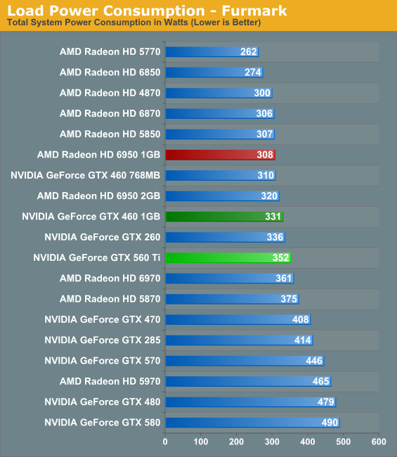
Under FurMark the gap between the GTX 460 1GB and GTX 560 Ti shrinks some, even after we disable the GTX 560 Ti’s overcurrent protection. It’s now a 21W gap, which is still more than we’d expect given NVIDIA’s official TDP numbers. Furthermore AMD’s PowerTune technology makes NVIDIA look quite bad here – the 200W capped 6950 1GB rig is drawing 44W less, and even the 6970 rig is only drawing 9W more. As we said when AMD first introduced PowerTune, we’re not against TDP-limited technologies so long as they’re done on a truly application-wide basis – so hopefully at some point we’ll see NVIDIA’s overcurrent protection technology evolve in to something closer to PowerTune instead of something that merely targets 2 of many stress testing applications.
The ultimate lesson from this however is that it once more reiterates the importance of good case cooling when using open-ended cards that don’t fully exhaust their hot air, such as the GTX 460 and GTX 560. Our airy GPU test bed has no problem with these cards, but at the end of the day you’re looking at 200W of heat and only around half of which is getting blown out of the case, leaving another 100W for the case to deal with. It’s a reasonable design choice on NVIDIA’s part, but it means you need to use the right case for the job. The GTX 560 Ti makes this all the more important, and I suspect we may be at the limits of what’s practical for a non-blower card.
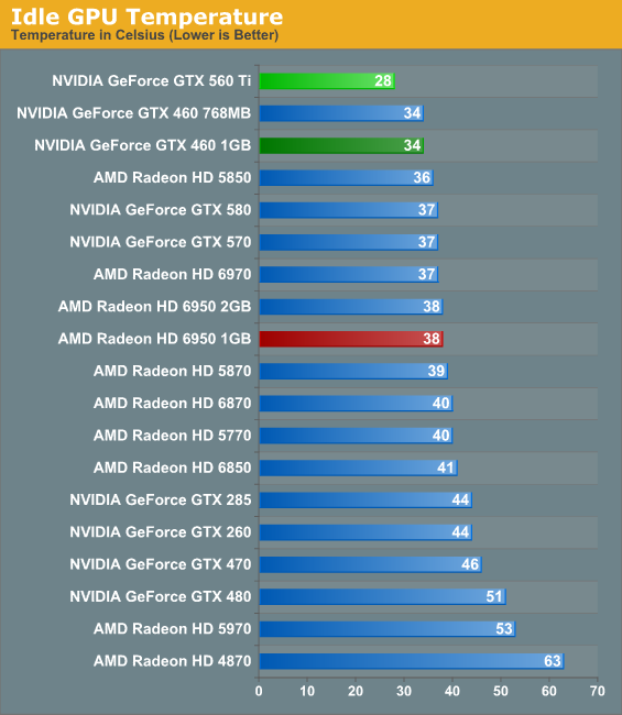
What do you get when you combine a large, open-air video card with an equally large and airy GPU test rig? Very, very low idle temperatures. Last year the GTX 460 set a new mark on our rig at 34C for idle, but with a bigger cooler and similar idle power consumption numbers, the GTX 560 Ti takes this one step farther. At 28C not only is the GTX 560 Ti several degrees cooler than the aforementioned GTX 560s, but it’s also only several degrees off of room temperature. This is something a blower design such as the GTX 570 or Radeon HD 6950 simply cannot match, even if idle power consumption is similar.
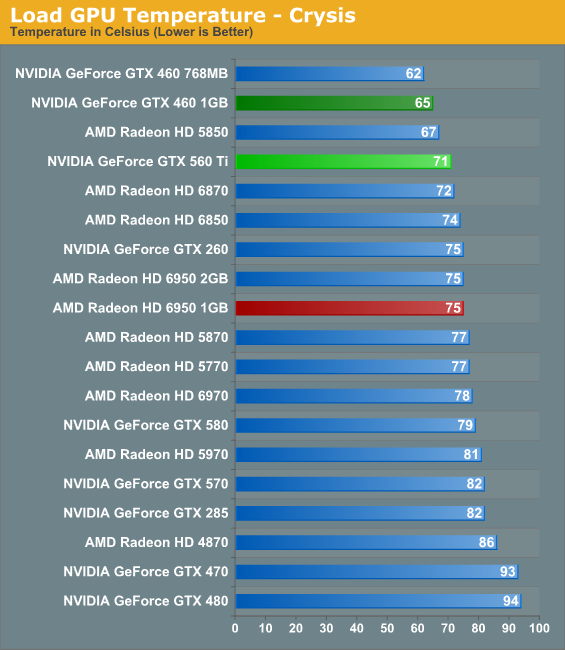
Compared to idle things end up being a little less rosy for the GTX 560 Ti, but they still look good. Even with a bigger cooler the GTX 560 cannot match the GTX 460s, but it’s doing fairly well against everything else. The open-air design still gives it an advantage versus blowers, but not by quite as much – the 6950 is only 4C off. Given that we figure the actual power consumption of the GTX 560 Ti is around 20W more than the GTX 460 1GB, it looks like the GTX 560 Ti’s cooler can’t fully make up for the additional heat the GTX 560 Ti’s GPU puts off.
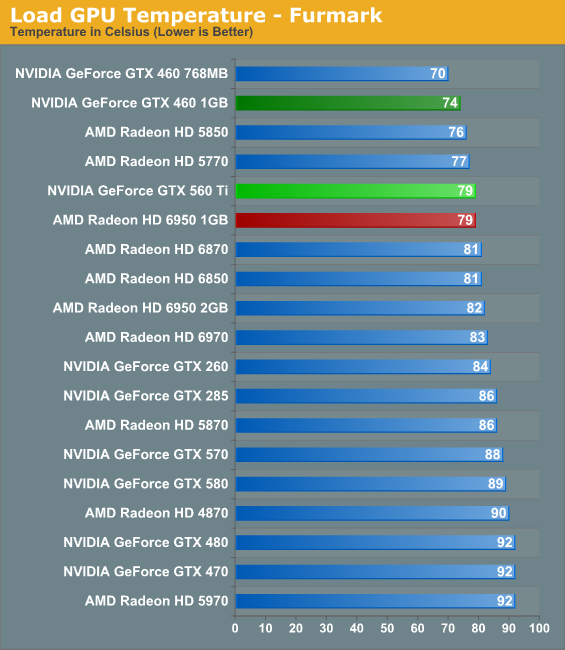
Under FurMark the story is quite similar. The GTX 560 Ti again is several degrees warmer than the GTX 460, and AMD’s blowers do start catching up thanks to PowerTune. Otherwise at 79C the card still runs quite cool, merely not as cool as the GTX 460 before it. When we get to our noise data however, we’ll see that NVIDIA may have optimized the GTX 560 for noise ahead of temperatures more than they did the GTX 460.
With that said, based on our numbers and TDP estimations though, we’re all the more curious at just how much case cooling is necessary for the GTX 560, and if it’s going to be as flexible as the GTX 460. It may be worth building a secondary GPU test rig with poor ventilation to see if the GTX 560 Ti is still suitable under sub-optimal conditions.
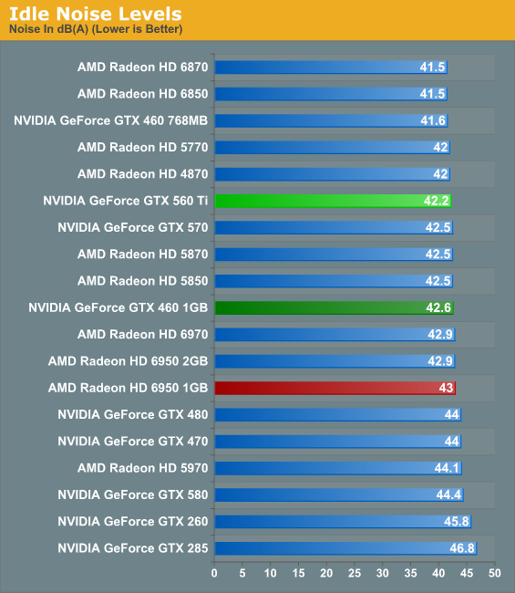
At idle virtually all of our cards run up against the noise floor, so there’s little to be surprised about here. The GTX 560 Ti is effectively as good as everything else.
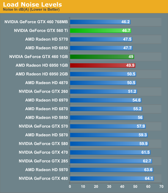
It’s our load noise values that make us reconsider our earlier temperature data. While the GTX 560 Ti may run hotter than a GTX 460, NVIDIA clearly didn’t lose their knack when it comes to noise. The GTX 460 768MB set a new record for a mid-range card, and the GTX 560 Ti is the second –best, besting even the GTX 460 1GB by a bit over 2dB. When it comes to our GPU testbed the GTX 560 is just shy of silent, which is quite an accomplishment for as much power as it consumes. This also handily illustrates why we don’t consider the Radeon HD 6870 to be much competition for the GTX 560 Ti – it may be cheaper, but it’s also a heck of a lot louder. It takes a 6950 to find an AMD card with similar performance that has acoustic qualities in the same neighborhood.
Final Thoughts
Wrapping things up, for the last week now I’ve been spending a considerable amount of time going over two thoughts: 1) What do I make of the GTX 560 Ti, and 2) What do I make of the name? The latter may sound silly, but I’m almost positive it’s the more important question. After all, why would NVIDIA resurrect the Ti suffix after an 8 year absence?
The answer I believe is a matter of momentum. There was a reason we called the GTX 460 the $200 King at its introduction: it was an aggressively priced card that shifted the market overnight, delivering a very high quality midrange card to a market that AMD failed to hit during their reign as the king. With a number of very quick price drops following its launch, it quickly became the $200 card of choice until AMD could fire back with the Radeon HD 6800 series. I would not classify it as the kind of legendary card that NVIDIA’s Ti 4200 became, but it had a good shot at it.
NVIDIA is now faced with a question of how they should follow-up on the GTX 460 only 6 months later. It would be difficult to recreate the GTX 460’s launch at this time – the market doesn’t have any gaping holes and NVIDIA does not have a brand-new chip. But NVIDIA wants to recreate July of 2010 anyhow – and with any luck April of 2002 while they’re at it. And that is why we have Ti.
To get a 30% performance improvement out of what’s fundamentally the same GPU is quite an accomplishment. I do not believe NVIDIA was originally intending for it to be this way (rather they’d launch something like the 560 back in July of 2010), but the result is nevertheless remarkable. Since the launch of the GTX 460 NVIDIA’s launches have been mostly solid, and the GTX 560 Ti adds to that list. Price/performance is not quite as aggressive as the GTX 460, but NVIDIA is still being aggressive enough to reshape the market – why else are we seeing Radeon HD 6800s for so cheap, and the very sudden launch of the 1GB Radeon HD 6950?
So what do I make of the GTX 560 Ti? There’s the question I haven’t quite answered. It seems like the video cards that go down in history as being truly great are aggressively priced cards the competition has no immediate answer for. I firmly believe that NVIDIA deserves most of the credit for the recent shakeup in video card pricing between $200 and $300 due to the launch of the GTX 560 Ti. But credit is not the same as a solid recommendation.
AMD’s scramble to launch the Radeon HD 6950 1GB has produced a card with similar levels of performance and pricing as the GTX 560 Ti, making it impossible to just blindly recommend the GTX 560 Ti. With sufficient case cooling both the GTX 560 and the Radeon HD 6950 1GB are good cards for the price, and represent a meaningful step up from where we were just 2 weeks ago. Ultimately I think the situation is very similar to December’s launch of the 6900 series, and the match-up between the GTX 570 and the Radeon HD 6970: we have two very similar cards in almost all respects. The GTX 560 Ti ultimately has the edge: it’s a bit faster and it’s quieter than the 6950, and if that’s all you care about then there’s the answer you seek. But you could grab the 6950 1GB and you’d be doing no worse. The deciding factor seems to come down to just how much to value noise and cooling (560) versus power consumption (6950), what games you play, and whether you’re currently invested in the NVIDIA (CUDA, 3D Vision) or AMD (Eyefinity) ecosystem.
In the long run I suspect pricing pressures will make things clearer. Based on what we’ve seen with the GTX 460, NVIDIA clearly has more pricing latitude than AMD with products in this range and with GPUs between 300mm2 and 400mm2. A stalemate is only 1 price drop away from being a clear victory for NVIDIA, so it may simply come down to just how badly NVIDIA wants to win.

