Original Link: https://www.anandtech.com/show/13584/nvidia-xavier-agx-hands-on-carmel-and-more
Investigating NVIDIA's Jetson AGX: A Look at Xavier and Its Carmel Cores
by Andrei Frumusanu on January 4, 2019 11:00 AM EST- Posted in
- SoCs
- NVIDIA
- Xavier
- Automotive
- Jetson
- Jetson AGX
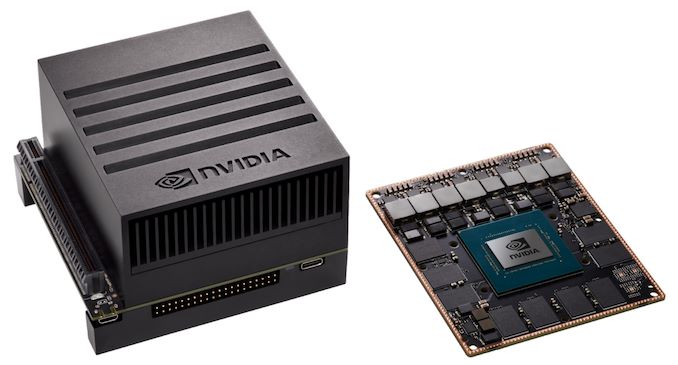
Today’s piece is a bit of an unusual review; NVIDIA’s new Jetson AGX embedded system kit isn’t really a device platform we’re expecting the average reader to think about, much less buy. NVIDIA’s shift over the last few years from offering consumer grade Tegra chipsets to more specialised silicon applications isn’t any more evident than in the new Tegra Xavier which powers the Jetson AGX. While the board's capabilities certainly fall outside of the use-cases of most consumers, it still represents a very interesting platform with a lot of functionality and silicon IP that we don’t find in any other device to this day. So when NVIDIA reached out to offer us a sample, we decided to have a go at assembling a high-level overview of what the board and the new Xavier chip can do.
First of all, we have to describe what this actually is. The Jetson AGX is a full-fledged small form-factor computer / embedded system, with the form of the whole unit not any bigger than 105x105mm. The AGX module itself is designed to be a complete commercial off the shelf (COTS) system for use in finished products, with NVIDIA aiming it at AI (read: neural networking) centric use cases such as robotics and industrial automation. Jetson boards typically occupy the small-to-mid volume end of the market, showing up in one-off products and items with limited production runs, where it doesn't make sense for a manufacturer to develop and deploy their own custom hardware.
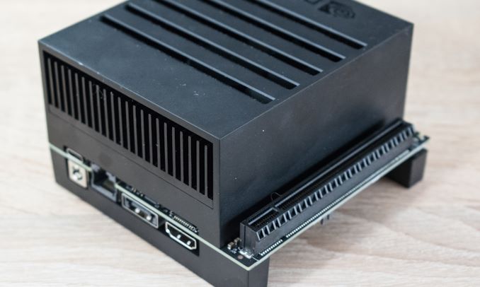
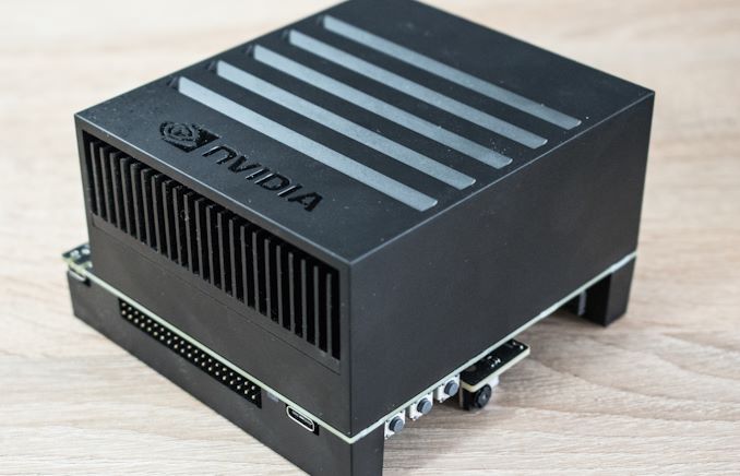
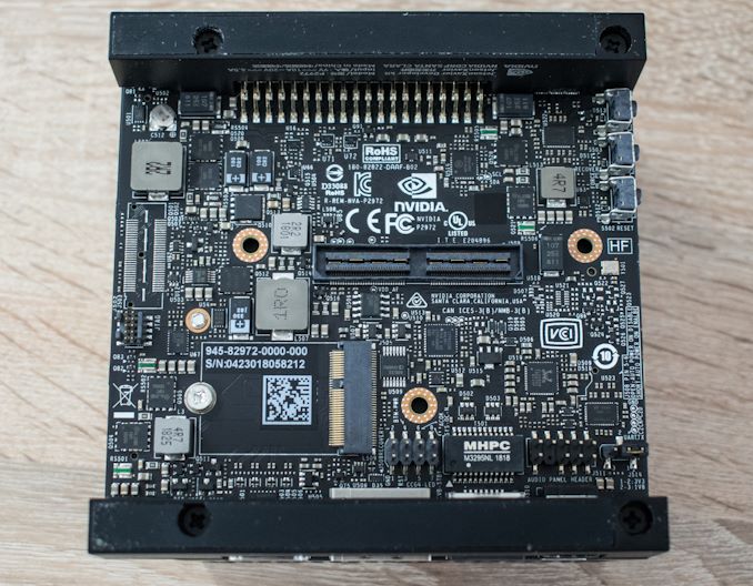
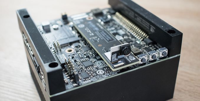
But of course the bare module is only half the story. You can't do development against a bare module, and this is where NVIDIA's complete Jetson AGX development kit comes in. The AGX dev kit comes with everything needed to run a single module, including a power supply, a heatsink, and more important of all, a breakout board. The breakout board offers various I/O headers and ports, ranging from your standard double USB-C 3.1 ports, HDMI connectors and Gigabit Ethernet ports, to more specialised connectivity such as MIPI CSI-2 connectors for camera connectivity and a range of typical development board headers such as a 40 pin GPIO connector.
The more unusual connectivity options of the Jetson AGX are the PCIe Gen4 x16 slot as well as a M.2 PCIe x1 extension slot that is meant to be used for connectivity add-ons such as WiFi or cellular modules, both features that aren’t common among Arm development board as most SoCs don’t have the spare PCIe controllers.
The board comes with many other connectors, and that’s one regard in which the new Jetson AGX doesn’t lack at all in flexibility. Power is supplied by an external generic 19V power supply – the stock one supplied by NVIDIA is a 65W LiteOn unit that seems no different than most laptop charger bricks.
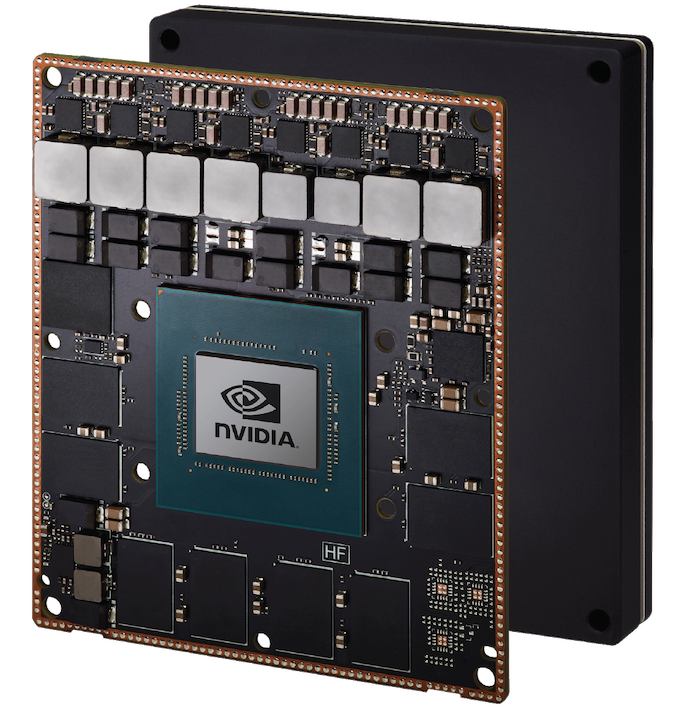
Underneath the quite heavy and solid aluminium heatsink we find what actually powers the Jetson AGX board: the AGX Xavier module. This is a system module that sits on top of the Jetson motherboard – the module has no I/O ports by itself and merely serves as the brains of the system, integrating the core components surrounding the Xavier chip, such as the 16GB of LPDDR4x memory, a small 32GB eMMC storage chip as well as all the power delivery circuits for powering the different power rails of the DRAM as well as IP blocks of the Xavier SoC.
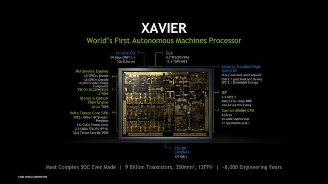
The Xavier chip, as said, is the brains of the platform and represents NVIDIA’s biggest and most complex SoC to date. With 9 billion transistors on a die size of 350mm², it’s among one of the heavyweights of the Arm ecosystem, although between its initial announcements and today Apple has one-upped NVIDIA in terms of transistor count as the new A12X is a 10B chip – in a much smaller manufacturing node.
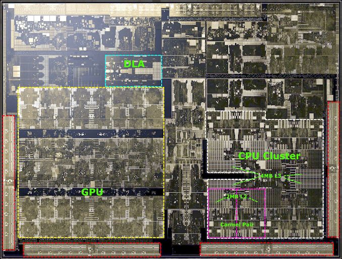
Coming from the traditional PC industry, NVIDIA doesn’t shy away from showing die shots of their products, which is something that is quite rare these days among the Arm SoC vendors. The Xavier SoC is mainly dominated by two big IP blocks which consist of the majority of the space allocated on the die: The 8-core “Carmel” CPU complex as well as a four-cluster Volta GPU.
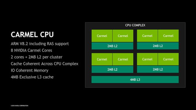
At the high level, the CPU complex contains 8 Carmel CPU cores configured in four clusters, each with a pair of Carmel CPU cores. Each cluster has an independent clock plane and shares a 2MB cache among two CPU cores. At the higher CPU complex level we find a 4MB L3 cache serving all clusters. We don’t know too much about the microarchitecture of the new Carmel cores - seemingly this looks to be a successor to NVIDIA’s Denver µarch, a design that was characterised by its dynamic code optimisation capability. The only thing that NVIDIA does advertise is that this is a 10-wide superscalar machine (10 execution ports in this case, not 10-wide decode) and has support for the ARMv8.2+RAS instruction set. We’ll come back to the CPU core later in the article.
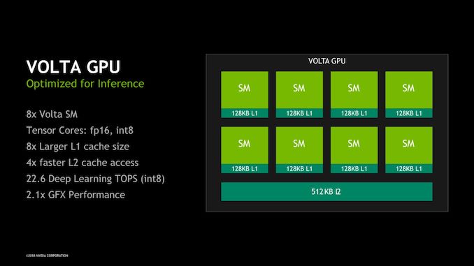
The GPU in Xavier has its roots in the Volta architecture. Here we find the GPU configured into four TPC (Texture processing clusters), each with two SMs (Stream multiprocessors), for a total of 8 SMs or 512 ALU lanes/CUDA cores. A most interesting aspect of the GPU is that because it is based on Volta, it also inherits the Tensor processing units from its bigger brethren. This augments the total processing power of the GPU by up to 22.6 8-bit TOPs or 11.3 FP16 TOPS on the part of the Tensor cores, on top of the respectively 2.8 and 1.4 TFLOPs for FP16 and FP32 CUDA operations provided by the SMs.
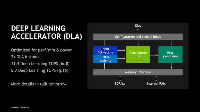
Alongside the CPU and GPU there’s many other important blocks, many of which NVIDIA had covered already at its HotChips 2018 presentation last summer. The one block that really does augment the Xavier SoC is the new DLA IP block: this is very much a new type of block that follows the trend we’ve seen in the mobile SoC space – a dedicated machine inferencing acceleration unit not unlike that which we’ve seen from the likes of HiSilicon or Apple. NVIDIA’s DLA promises performances of up to 11.4 int8 TOPS and is also capable of FP16 operation at half speed at 5.7 TOPS. On the SoC, the unit is implemented as a dual-core instance.
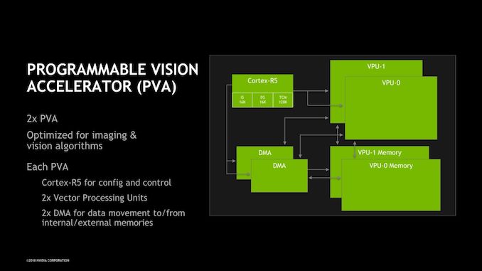
Alongside the DLA, the programmable vision accelerator is again a key component of the Xavier system that allows it focus on vision and in particular robotics, embedded AI and automotive use-cases. The PVA is a more traditional vision IP block that handles more rudimentary tasks such as object detections in a much more efficient way than it would be able to be handled by the GPU or machine inferencing algorithms. Here the PVA will be the first IP block after the ISP in the vision pipeline that will serve to segment parts of an image into objects that will be then forwarded to other algorithms that then would happen on the GPU or DLA.
Machine Inference Performance
The core aspects of the Xavier platform are its machine inferencing performance characteristics. The Volta GPU alongside the DLA core represent significant processing power in a compact and low-power platform.
To demonstrate the machine learning inference prowess of the system, NVIDIA provides the Jetson boards with a slew of software development kits as well as hand-tuned frameworks. The TensorRT framework in particular does a lot of heavy lifting for developers and represents the main API through which the GPU’s Tensor units as well as the DLA will be taken advantage of.
NVIDIA prepared a set of popular ML models for us to test out, and we’d be able to precisely configure the models in terms of how they were run on the platform. All the models running on the GPU and its Tensor core were able to run at either quantized INT8 forms, or in FP16 or FP32 forms. The batch sizes were also configurable, but we’ve kept it simple at just showcasing the results with a batch size of 32 images as NVIDIA claims this is the more representative use-case for autonomous machines.
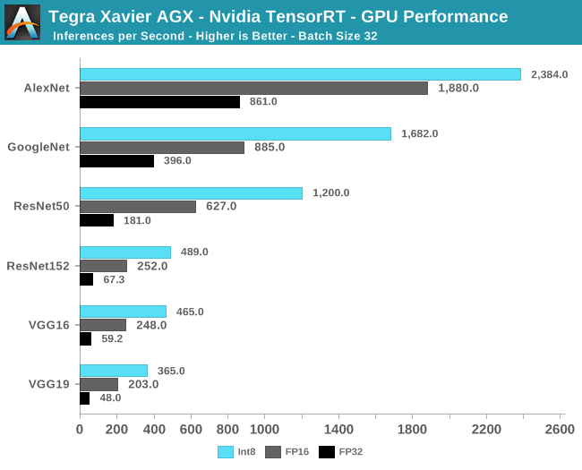
The results of the GPU benchmarks are a bit esoteric because we have few comparison points against which we can evaluate the performance of the AGX. Among the more clear results we see here is that the inferencing performance in absolute terms is reaching rather high rates, particularly in the INT8 and FP16 modes, representing sufficient performance to run a variety of inferencing tasks on a large number of input sets per second. The only real figure we can compare to anything in the mobile market is the VGG16 results compared to the AImark results in our most recent iPhone XS review, where Apple’s new NPU scored a performance of 39 inferences/second.
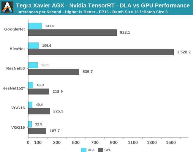
NVIDIA also made it possible to benchmark the DLA blocks, however this came with some caveats: The current version of the TensorRT framework was still a bit immature and thus doesn’t currently allow for running the models in INT8 mode, forcing us to resort to comparisons in FP16 mode. Furthermore I wasn’t able to run the tests with the same large batch size as on the GPU, so I’ve reverted to using smaller sizes of 16 and 8 where appropriate. Smaller batch sizes have more overhead as it takes proportionally longer time on the API side of things and less actual processing time on the hardware.
The performance of the DLA blocks at first glance seems a bit disappointing, as their performance is just a fraction of what the Volta GPU is able to showcase. However raw performance isn’t the main task of the DLA, it serves as a specialized offloading block which is able to operate at higher efficiency points than the GPU. Unfortunately, I wasn’t able to directly measure the power differences between the GPU and the DLA, as introducing my power measurement equipment into the DC power input of the board led to system instabilities, particularly during the current spikes when the benchmarks were launching their workloads. The GPU inference workloads did see the board power reach around ~45W while in its peak performance mode.
NVIDIA's VisionWorks Demos
All the talk about the machine vision and inferencing capabilities of the platform can be something that’s very hard to grasp if you don’t have a more intimate knowledge of the use-cases in the industry. Luckily, NVIDIA’s VisionWorks SDK comes with a slew of example demos and source code projects that one can use as a baseline for one’s commercial applications. Compiling the demos was a breeze as everything was set up for us on the review platform.
Alongside the demo videos, I also opted to showcase the power consumption of the Jetson AGX board. Here we’re measuring the power of the platform at the 19V DC power input with the board at its maximum unlimited performance mode. I had board’s own fan disabled (it can be annoyingly loud) and instead used an externally-powered 120mm bench fan blowing onto the kit. At a baseline power level, the board used ~8.7-9W while sitting idle and actively outputting to a 1080p screen via HDMI while also being connected to Gigabit Ethernet.
The first demo showcases the AGX’s feature tracking capabilities. The input source is a pre-recorded video to facilitate testing. While the video output was limited to 30fps, the algorithm was running in excess of 2-300fps. I did see quite a wide range of jitter in the algorithm fps, although this could be attributed to scheduling noise due to the low duration of the workload while in a limited FPS output mode. In terms of power, we see total system consumption hover around 14W, representing an active power increase of 5W above idle.
The second demo is an application of a Hough transform filter which serves as a feature extraction algorithm for further image analysis. Similarly to the first demo, the algorithm can run at a very high framerate on a single stream, but usually we’d expect a real use-case to use multiple input streams. Power consumption again is in the 14W range for the platform with an average active power of ~4.5W.
The motion estimation demo determines motion vectors of moving objects in a stream, a relatively straightforward use-case in automotive applications.
The fourth VisionWorks demo is the computational implementation of EIS (Electronic image stabilisation), were given an input video stream the system will crop out margins of the frame and use this space as the stabilisation window in which the resulting output stream will be able to elastically bounce against, reducing smaller juddery motions.
Finally, the most impressive demo which NVIDIA provided was the “DeepStream” demo. Here we see a total of 25 720p video input streams played back all simultaneously all while the system is performing basic object detection in every single one of them. This workload represented a much more realistic heavy use-case being able to take advantage of the processing power of the AGX module. As you might expect, power consumption of the board also rose dramatically, averaging around 40W (31W active work).
NVIDIA's Carmel CPU Core - SPEC2006 Speed
While the Xavier’s vision and machine processing capabilities are definitely interesting, it’s use-cases will be largely out-of-scope for the average AnandTech reader. One of the aspects of the chip that I was personally more interested in was NVIDIA’s newest generation Carmel CPU cores, as it represents one of the rare custom Arm CPU efforts in the industry.
Memory Latency
Before going into the SPEC2006 results, I wanted to see how NVIDIA’s memory subsystem compares against some comparable platform in the Arm space.
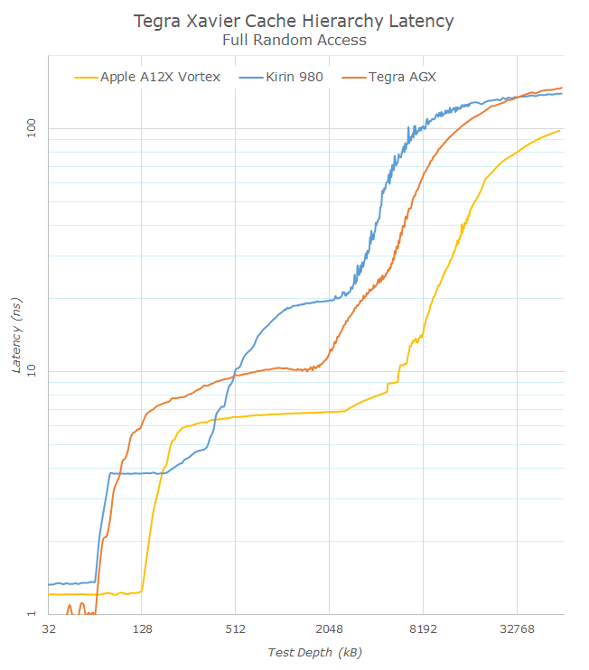
In the first logarithmic latency graph, we see the exaggerated latency curves which make it easy to determine the various cache hierarchy levels of the systems. As NVIDIA advertises, we see the 64KB L1D cache of the Carmel cores. What is interesting here is that NVIDIA is able to achieve quite a high performance L1 implementation with just under 1ns access times, representing a 2-cycle access which is quite uncommon. The second hierarchy cache is the L2 that continues on to the 2MB depth, after which we see the 4MB L3 cache. The L3 cache here looks to be of a non-uniform-access design as its latency steadily rises the further we go.
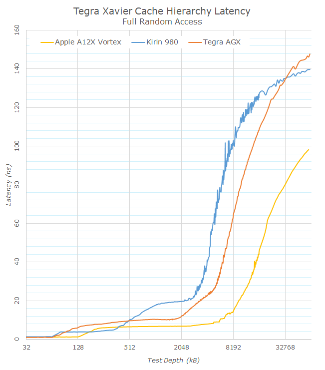
Switching back to a linear graph, NVIDIA does have a latency advantage over Arm’s Cortex-A76 and the DSU L3 of the Kirin 980, however it loses out at deeper test depths and latencies at the memory controller level. The Xavier SoC comes with 8x 32bit (256bit total) LPDDR4X memory controller channels, representing a peak bandwidth of 137GB/s, significantly higher than the 64 or 128bit interfaces on the Kirin 980 or the Apple A12X. Apple overall still has an enormous memory latency advantage over the competition as its massive 8MB L2 cache as well as the 8MB SLC (System level cache) allows for significant lower latencies across all test depths.
SPEC2006 Speed Results
A rarity for whenever we're looking at Arm SoCs and products built around them, NVIDIA’s Jetson AGX comes with a custom image for Ubuntu Linux (18.04 LTS). On one hand, including a Linux OS gives us a lot of flexibility in terms of test platform tools; but on the other hand, it also shows the relatively immaturity of Arm on Linux. One of the more regretful aspects of Arm on Linux is browser performance; to date the available browsers are still lacking optimised Javascript JIT engines, resulting in performance that is far worse than any commodity mobile device.
While we can’t really test our usual web workloads, we do have the flexibility of Linux to just simply compile whatever we want. In this case we’re continuing our use of SPEC2006 as we have a relatively established set of figures on all relevant competing ARMv8 cores.
To best mimic the setup of the iOS and Android harnesses, we chose the Clang 8.0.0 compiler. To keep things simple, we didn’t use any special flags other than –Ofast and a scheduling model targeting the Cortex-A53 (It performed overall better than no model or A57 targets). We also have to remind readers that SPEC2006 has been retired in favour of SPEC2017, and that the results published here are not officially submitted scores, rather internal figures that we have to describe as estimates.
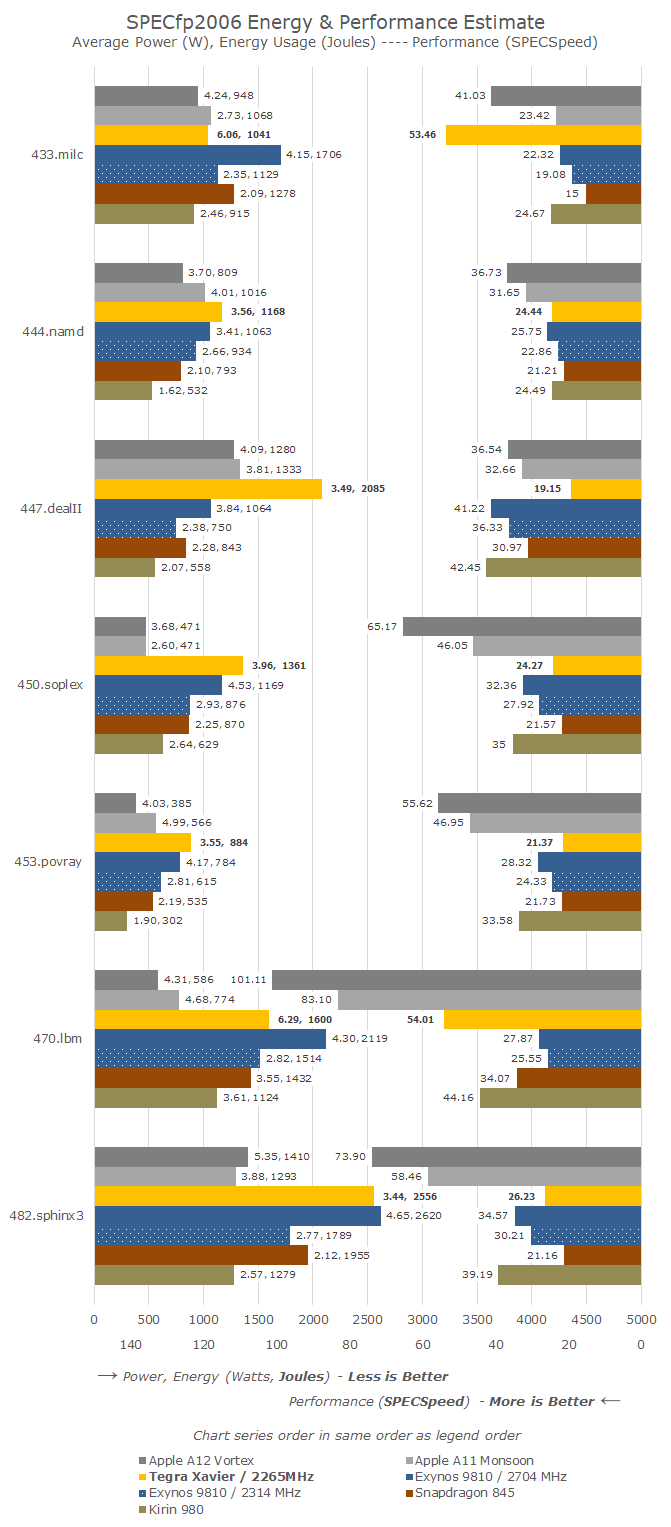
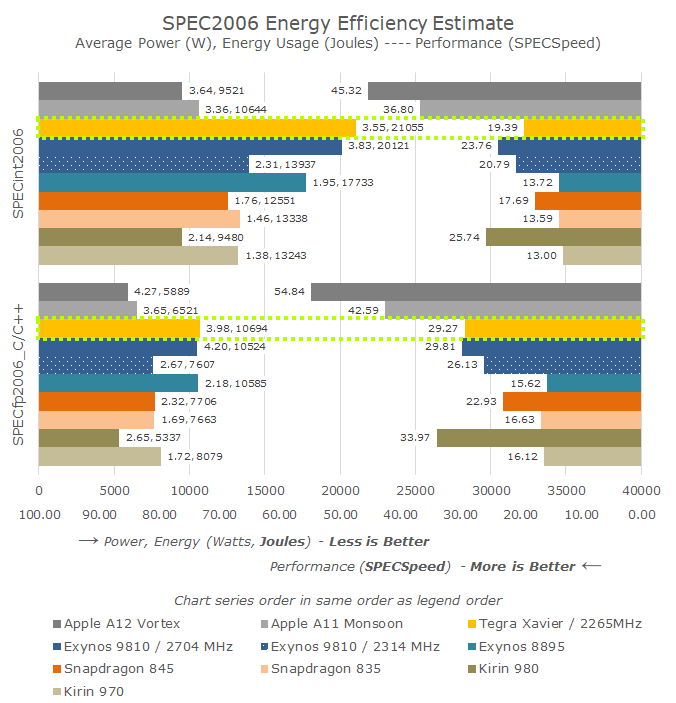
The power efficiency figures presented for the AGX, much like all other mobile platforms, represent the active workload power usage of the system. This means we’re measuring the total system power under a workload, and subtracting the idle power of the system under similar circumstances. The Jetson AGX has a relatively high idle power consumption of 8.92W in this scenario, much that can be simply be attributed from a relatively non-power optimised board as well as the fact that we’re actively outputting via HDMI while having the board connected to GbE.
In the integer workloads, the Carmel CPU cores' performance is quite average. Overall, the performance across most workloads is extremely similar to that of Arm’s Cortex-A75 inside the Snapdragon 845, with the only outlier being 462.libquantum which showcases larger gains due to Xavier’s increased memory bandwidth.
In terms of power and efficiency, the NVIDIA Carmel cores again aren’t quite the best. The fact that the Xavier module is targeted at a totally different industry means that its power delivery possibly isn’t quite as power optimised as on a mobile device. We also must not forget that the Xavier has an inherent technical disadvantage of being manufactured on a 12FFN TSMC process node, which should be lagging behind Samsung’s 10LPP processes of the Exynos 9810 and the Snapdragon 845, and most certainly represents a major disadvantage against the newer 7nm Kirin 980 and Apple A12.
On the floating point benchmarks, Xavier fares overall better because some of the benchmarks are characterised by their sensitivity to the memory subsystem; in 433.milc this is most obvious. 470.lbm also sees the Carmel cores perform relatively well. In the other workloads however, again we see Xavier having trouble to differentiate itself much from the performance of a Cortex A75.
Here’s a wider performance comparison across SPEC2006 workloads among the most recent and important ARMv8 CPU microarchitectures:
Overall, NVIDIA’s Carmel core seems like a big step up for NVIDIA and their in-house microarchitecture. However when compared against most recent cores from the competition, we see the new core having trouble able to really distinguish itself in terms of performance. Power efficiency of the AGX also lags behind, however this is something that was to be expected given the fact that the Jetson AGX is not a power optimised platform, beyond the fact that the chip’s 12FFN manufacturing process is a generation or two behind the latest mobile chips.
The one aspect which we can’t quantize NVIDIA’s Carmel cores is its features: This is a shipping CPU with ASIL-C functional safety features that we have in our hands today. The only competition in this regard would be Arm’s new Cortex A76AE, which we won’t see in silicon for at least another year or more. When taking this into account, it could possibly make sense for NVIDIA to have gone with its in-house designs, however as Arm starts to offer more designs for this space I’m having a bit of a hard time seeing a path forward in following generations after Xavier, as competitively, the Carmel cores don’t position themselves too well.
NVIDIA's Carmel CPU Core - SPEC2006 Rate
Something that we have a tough time testing on other platforms is the multi-threaded performance of CPUs. On mobile devices thermal constraints largely don’t allow these devices to showcase the true microarchitectural scaling characteristics of a platform, as it's not possible to maintain high clockspeeds. NVIDIA’s Jetson AGX dev kit doesn’t have these issues thanks to its oversized cooler, and this makes it a fantastic opportunity to test out Xavier's eight Carmel cores, as all are able to run at peak frequency without worries about thermals (in our test bench scenario).
SPEC2006 Rate uses the same workloads as the Speed benchmarks, with the only difference being that we’re launching more instances (processes) simultaneously.
Starting off with SPECin2006 rate:
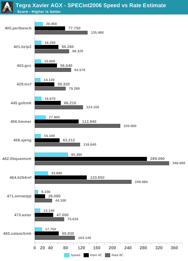
The way that SPEC2006 rate scores are calculated is that it measures the execution time of all instances and uses the same reference time scale as the Speed score- with the only difference here being is that the final score is multiplied by the amount of instances.
I chose to run the rate benchmarks with both 4 and 8 instances to showcase the particularity of NVIDIA’s Carmel CPU core configuration. Here we see the four core run perform roughly as expected, however the eight core run scores are a bit less than you’d expect. To showcase this better, let’s compare the scaling factor in relation to the single-core Speed results:
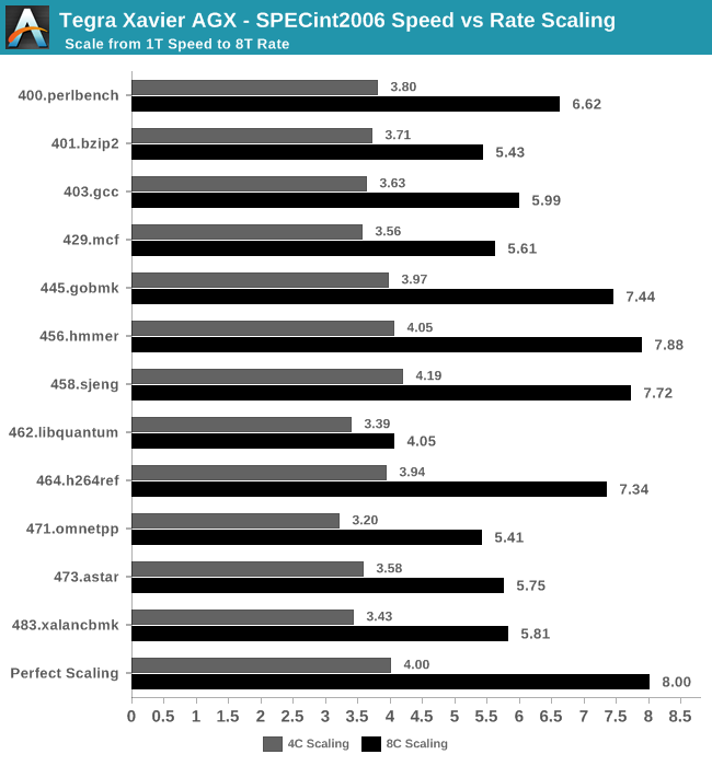
The majority of the 4C workloads scaling near the optimal 4x factor that we’d come to expect, with only a few exceptions having a little worse performance scaling figures. The 8C workloads however showcase significantly worse performance scaling factors, and it’s here where things get interesting:
Because Xavier’s CPU complex consists of four CPU clusters, each with a pair of Carmel cores and 2MB L2 cache shared among each pair, we have a scenario where the CPU cores can be resource constrained. In fact, by default what the kernel scheduler on the AGX does is to try to populate one core within all clusters first, before it schedules anything on the secondary cores within a cluster.
In effect what this means that in the 4C rate scenarios, each core within a cluster essentially has exclusive use of the 2MB L2 cache, while on the 8C rate workloads, the L2 cache has to be actively shared among the two cores, resulting in resource contention and worse performance per core.
The only workloads that aren’t nearly as affected by this, are the workloads which are largely execution unit bound and put less stress on the data plane of the CPU complex, this can be seen in the great scaling of some workloads such as 456.hmmer for example. On the opposite end, workloads such as 462.libquantum suffer dramatically under this kind of CPU setup, and the CPU cores are severely bandwidth starved and can’t process things any faster than if there were just one core per cluster active.
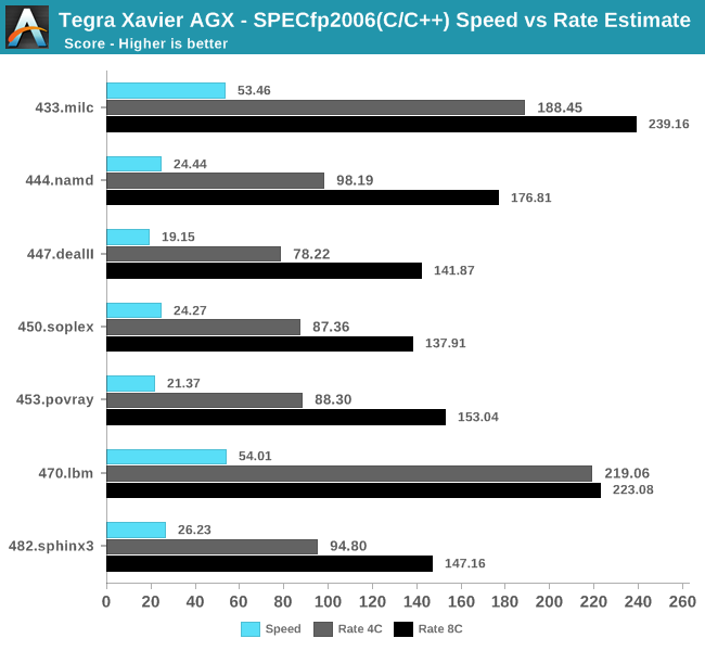
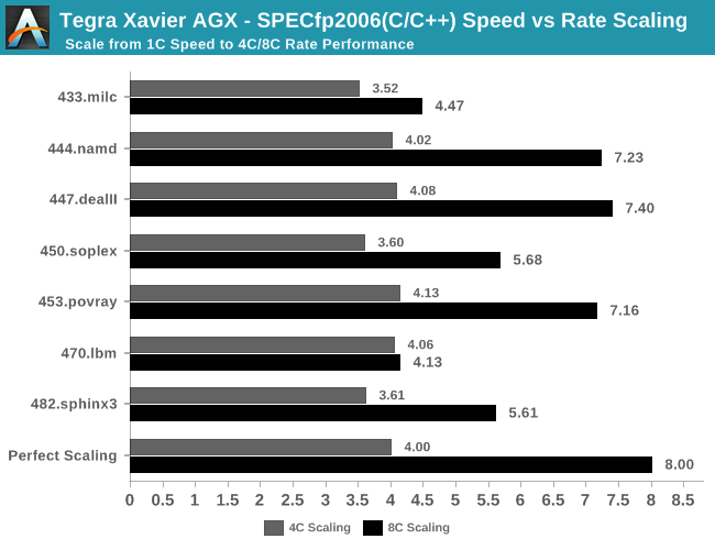
The same analysis can be applied to the floating point rate benchmarks: Some of the less memory sensitive workloads don’t have all that much issue in scaling well with core counts, however others such as 433.milc and 470.lbm again showcase quite bad performance figures when run on all cores on the system.
Overall, NVIDIA's design choices for Xavier’s CPU cluster are quite peculiar. It’s possible that NVIDIA either sees a majority of workloads targeted on the AGX to not be an issue in terms of their scaling, or actual use of the platform in automotive use-cases we would see each core in a cluster operating in lock-step with each other, theoretically eliminating possible resource contention issues on the level of the shared L2 cache.
I didn’t get to measure full power figures for all rate benchmarks, but in general the power of an additional core within a separate cluster will scale near linearly with the power figures of the previously discussed single-core Speed runs, meaning the 4-core rate benchmarks showcase active power usage of around ~12-15W. Because performance doesn’t scale linearly with the additional secondary cluster cores, the power increase was also more limited. Here I saw up to a total system power consumption of up to ~31W for workloads such as 456.hmmer (~22W active), while more bottlenecked workloads ran around ~21-25W for the total platform (~12-16W active).
Closing Thoughts
Usually at the end of an article we’d be coming to a conclusion. However as this piece is more of a hands-on, we'll limit our scope a bit. We're not really in a position to properly determine how Xavier stacks up in the robotics or automotive spaces, so that's going to have to remain a discussion for another time.
We had a quick, superficial look at what NVIDIA would be able to offer industrial and automotive costumers – in that regard Xavier certainly seems to offer a ton of flexibility and also significant raw processing power. It’s clear that the one aspect in which NVIDIA tries to promote Xavier the most is its vision and machine learning capabilities, and here, although we lack any great comparison points, it does look like NVIDIA is able to provide an outstandingly robust platform.
For most AnandTech readers, the most interesting aspect of the Jetson AGX and Xavier will be the new Carmel CPU cores. Although a deeper microarchitectural analysis of the core was out of the scope of this article, what does matter in the end is the resulting performance and power characteristics, which we did measure in detail. Here NVIDIA’s results landed in relatively modest territories, with Carmel landing at around, or slightly higher performance levels of an Arm Cortex-A75.
Multi-threaded performance of Xavier is great, although again the rather odd CPU cluster configuration can result in scenarios where not all eight cores are able to perform at their peak performance under some circumstances. As Arm tries to enter the automotive sector with dedicated IP, I do wonder if in the future it will make sense for NVIDIA to continue on with their rather exotic CPU microarchitecture.
The challenge to NVIDIA then is how to best stay ahead of Arm and the army of licensees that will be implementing their automotive-focused IP in the future. I think the one aspect where NVIDIA can offer a lot more value than competing products is the fact that NVIDIA is creating a strong software ecosystem and development toolkits, allowing customers to more easily achieve enable their product use-cases.
The Jetson AGX development kit costs a whopping $2500 (It can be attained for $1299 if you are part of Nvidia's development programme) – and even the individual modules are $1100 – making it non-viable for the hobbyist looking to use it as a server machine at home. But for companies looking to setup more complex systems requiring heavy vision processing, or actually deploying the AGX module in autonomous applicaitons for robotics or industrial uses, then Xavier looks quite interesting and is definitely a more approachable and open platform than what tends to exist from competing products.

