Intel Opens D1X-Mod3 Fab Expansion; Moves Up Intel 18A Manufacturing to H2’2024
by Ryan Smith on April 11, 2022 1:00 PM EST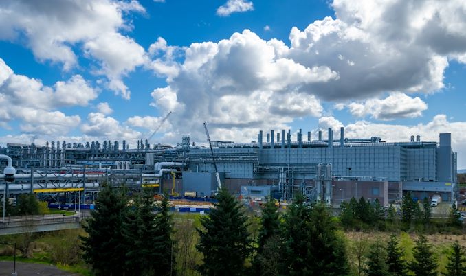
Intel for the last few years has been undergoing a major period of manufacturing expansion for the company. While the more recent announcements of new facilities in Ohio and Germany have understandably taken a lot of the spotlight – especially given their importance to Intel’s Foundry Services plans – Intel has been working even longer on expanding their existing facilities for their own use. The company’s development of next-generation EUV and Gate-All-Around-style transistors (RibbonFET) not only requires creating and refining the underlying technology, but it also just flat out requires more space. A lot of it.
To that end, Intel today is holding a grand opening in Oregon for the Mod3 expansion of D1X, the company’s primary development fab. The expansion, first announced back in 2019, is the third such mod (module) and second expansion for Intel’s main dev fab to be built since D1X’s initial construction in 2010. And in keeping with tradition for Intel fab launches and expansions, the company is making something of an event of it, including bringing Oregon’s governor out to show off their $3 Billion investment.
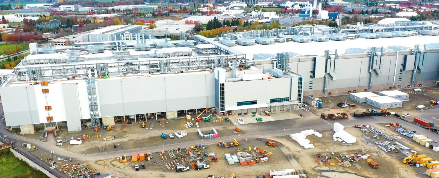
But fanfare aside, the latest mod for the fab is a genuinely important one for Intel: not only does it add a further 270,000 square feet of clean room space to the facility – expanding D1X by about 20% – but it’s the only fab module that’s big enough to support the High Numerical Aperture (High NA) EUV tool that Intel will be using starting with its 18A process. ASML’s forthcoming TWINSCAN EXE:5200 EUV tool is designed to be their most powerful yet, but it’s also quite a bit larger than the NXE 3000 series EUV tools Intel is using for their first generation EUV processes (Intel 4/Intel 3). It’s so big that D1X’s ceiling is too low to fit the machine, never mind the floor supporting its weight.
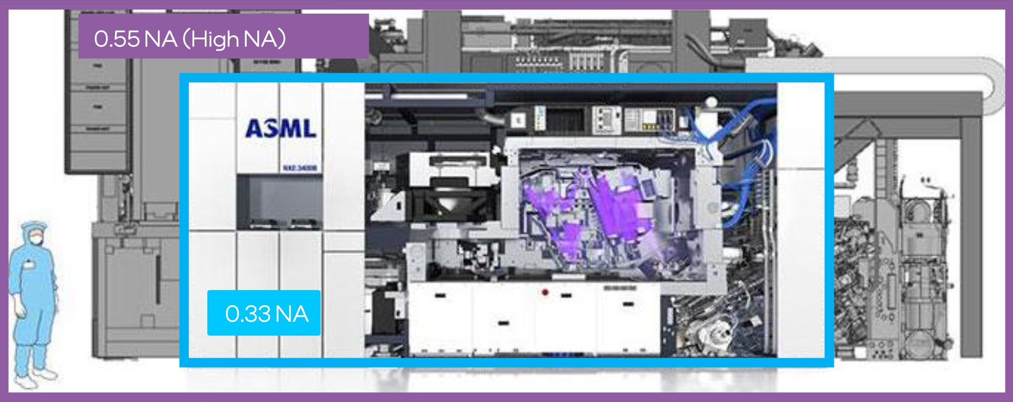
Size Comparison: ASML Normal & High NA EUV Machines
As a result, Mod3 has been built, in no small part, to fit this massive machine. Intel isn’t expecting to take delivery of the machine for a couple more years, but they had to start preparations years in advance just to get to this point.
Meanwhile, although D1X-Mod3 is only being officially declared open today, Intel has already been moving critical tools into Mod3 since last August. Consequently, today’s opening is something of a ceremonial launch for the mod, as parts of it are already setup (if not already in use). Still, even with that head start, according to Intel the company expects to be moving in tools for another year, especially as they bring in the remaining, lower-priority tools.
Coincidentally, our own Dr. Ian Cutress had a chance to see D1X in all of its glory late last year, when he toured the facility. At the time Intel was already in the final stages of finishing the Mod3 expansion, as well as bringing up EUV machines as part of the development of the Intel 4 and Intel 3 process nodes, Intel’s first EUV nodes. So for more information on D1X and what goes on there, be sure to check out that article.
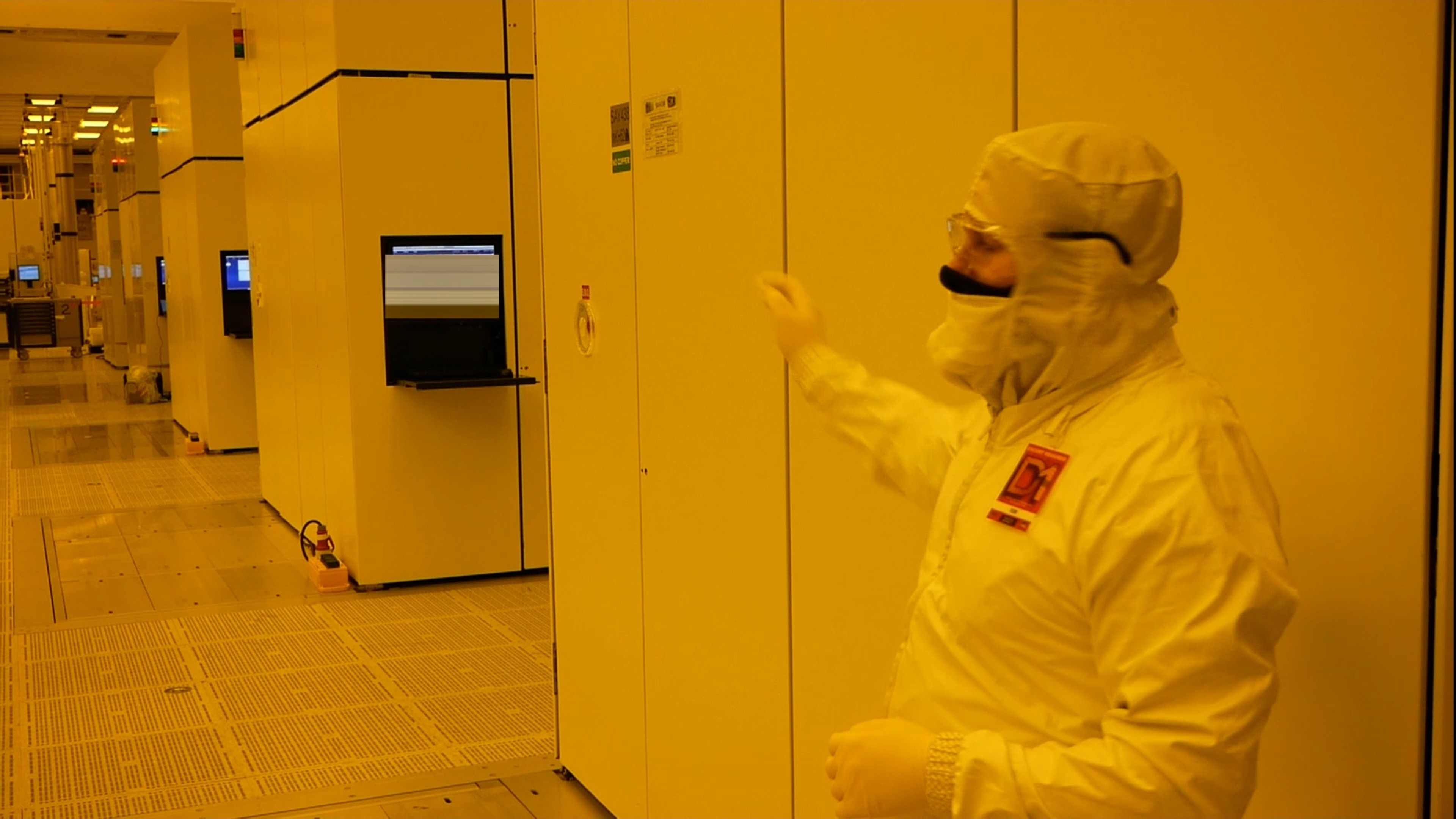
A line of EUV machines at D1X
Finally, along with formally opening the Mod3 expansion, Intel today is also using the opportunity to rename the 450-acre campus that D1X sits on. Intel’s Ronler Acres campus has been the center of Intel’s fab R&D efforts for decades, and along with D1X, also houses Intel’s older D1 development fabs, such as D1B, D1C, and D1D. So, in reflection of all of the important R&D that goes on at the site, Intel is renaming it after co-founder Gordon Moore, one of the instrumental figures behind the development of Intel’s earliest technologies. The newly renamed campus will now go by Gordon Moore Park at Ronler Acres, or Gordon Moore Park for short. And despite the many (many) things that have been named after Moore over the years, from laws and buildings to awards and medals, this is the largest thing named after Moore (yet), as it’s the first time a whole campus has been named after the luminary.

Intel Roadmap Update: Intel 18A Moved Up to H2 2024
Alongside briefing the press about the D1X-Mod3 opening, Intel also used their latest press event to get everyone up to speed on the latest updates on Intel’s development roadmap. Strictly speaking, nothing here is new – all of this was first announced during Intel’s 2022 Investor Meeting back in February. However this is the first time Intel has engaged the technical press, rather than investors, on the current state of its development efforts.
The big news here is that Intel is formally moving up the start date for manufacturing on the Intel 18A node. Intel’s second-generation “angstrom” node was originally expected in 2025; but now the company is bumping that up by half a year, to the second half of 2024.
As a result, Intel’s roadmap now looks like this:
With the company already gearing up for its first EUV process, Intel 4, later this year, Intel’s roadmap starts looking very compressed beginning in the second half of 2023. The second half of that year will see Intel 3 go into production, which is Intel’s enhanced EUV process. Meanwhile, potentially as soon as 6 months after that, Intel 20A goes into production. 20A is Intel’s first “angstrom” node, which incorporates their gate-all-around-style “RibbonFET” FinFets, as well as PowerVias.
But, if all goes according to plan, 20A will seemingly be a relatively short-lived node due to the movement of 18A. Intel’s second-generation angstrom node, which will incorporate an updated ribbon design and other improvements to Intel’s GAA manufacturing technology. Since 18A remains the farthest node out on Intel’s manufacturing roadmaps, the company is remaining relatively mum on everything new that 18A will entail, but it remains the point where Intel plans to re-establish unquestioned leadership of the chip making industry.
According to Intel, 18A development has been moving so well that the company’s R&D operations are now on or ahead of all of their development milestones, giving the company confidence that they can begin manufacturing products based on the process node in late 2024, instead of 2025 as first planned.
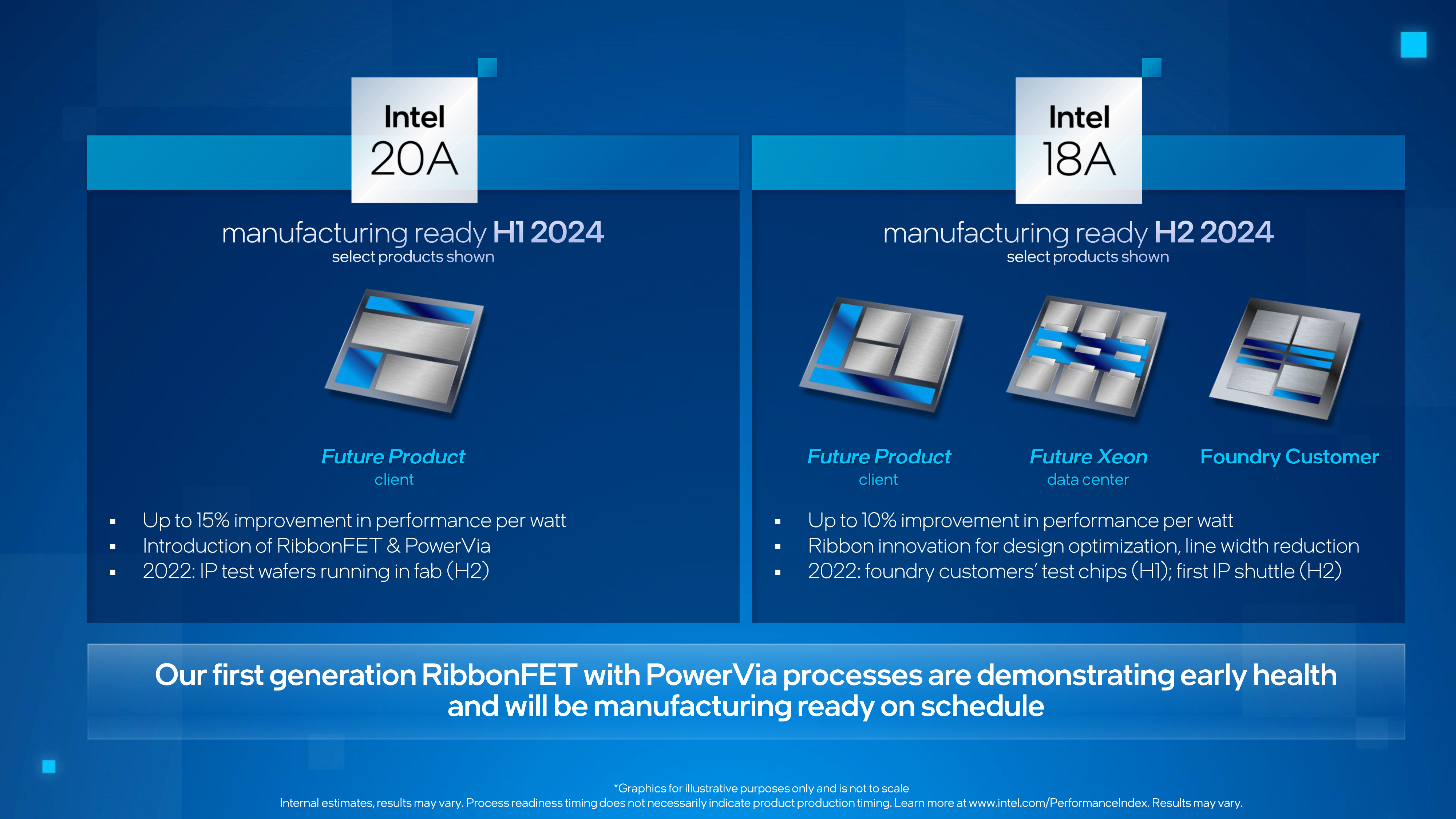
One consequence of bringing in 18A, however, is that it means Intel is now definitely going into initial production of 18A without all of their High NA machines. 18A remains the process node where High NA machines will debut, but as the TWINSCAN EXE 5200 is still not expected to be in place until 2025, that means Intel will now have to use their existing 3000 series machines to kickstart 18A production. Until this latest development, Intel had been presenting High NA machines and 18A as being tied at the hip, so whether that was always the actual case or not, now that is clearly not the case.
What that means for 18A production, in turns, remains to be seen. Since Intel can use their normal (non-HA) machines for 18A, then presumably the biggest advantages of the High NA machines were throughput, allowing Intel to process wafers with little (or not) multi-patterning thanks to High NA’s greater accuracy. Seemingly, the most likely outcome is that Intel will be able to produce 18A in 2024, and maybe even in decent volumes, but that they won’t be able to go into Intel-scale high volume manufacturing until the first High NA machine is available in 2025.
And, as always, it should be noted that Intel’s manufacturing roadmap dates are the earliest dates that a new process node goes into production, not the date that hardware based on the technology hits the shelves. So even if 18A launches in H2’24 as it’s now scheduled, it could very well be a few months into 2025 before the first products are in customer hands, especially if Intel launches in the later part of that window. All of which, given the large size of these launch windows and Intel’s own history, is a likely bet, as Intel has rarely launched new products/technologies early in a release window.
Finally, Intel’s development briefing also included confirmation that Intel is employing a purely internal “test risk reduction” node as part of their development process for their PowerVia technology. The purpose of the test node is to decouple the full risk of 20A by allowing Intel to develop and test PowerVias separately from RibbonFETs. In this case, the test node uses Intel’s well-established FinFET technology on the front-end, while employing a test version of PowerVia on the backend. No such node has been announced for RibbonFETs, but even if one doesn’t exist, not having to debug first-generation PowerVia on 20A alongside the RibbonFETs is still a simplification of the process, as it allows Intel to pursue both elements semi-independently, and learn from both of them in the process.

This is a significant change from how Intel has developed major new manufacturing nodes in the past, and even they are the first to admit as such. Intel’s 10nm problems were caused in large part by bundling too many technology changes together all at once, combined with a very aggressive reduction in feature size. Separating these things into smaller, more frequent manufacturing node updates was one way Intel is mitigating this risk in the future. And now with an internal test node for PowerVia development, they’re aiming to do even more risk mitigation in order to be able to roll out both RibbonFETs and PowerVia together in the first half of 2024 as part of Intel 20A.


89 Comments
View All Comments
mode_13h - Tuesday, April 12, 2022 - link
> they will ship something on it in 2023Q3. But will it actually be a significant> change from the earlier node? And will the item shipped be of any relevance?
Yes, key questions. Many of us remember how they seemed to ship a few trays of Cannon Lake, just so they could tell investors they delivered on some revision of their 10 nm timeline.
> intel Arc ... That was going to ship Q1 2022.
Yes, March 30th was suspiciously close to the end of the quarter. Funny enough, "Intel shill" site Anandtech didn't even cover their launch announcement, unlike many other tech sites.
> Now apply that same outcome to this process roadmap/fantasy...
Comparing manufacturing process to a graphics product is not really apples-to-apples.
For me, the elephant in the room is still Intel's 10 nm debacle. That's reason enough to doubt everything Intel says about their manufacturing tech.
Calin - Tuesday, April 12, 2022 - link
"I'm sure Intel will have a node CALLED 18A"Intel was pretty honest until now with the 14nm, 14+, 14++, ...
wumpus - Saturday, May 7, 2022 - link
They may have been more honest about 14nm, 14+, 14++ but their schedules and roadmaps were pure fantasy for years (going back to the transition to 14nm). And this article is all about the "new improved marketing" of the schedule.Spunjji - Wednesday, April 13, 2022 - link
I remain sceptical for similar reasons.JayNor - Monday, April 11, 2022 - link
Intel responded to the Optane rumors. Gen 3 optane is still on its way. They also added optane support to the new agilex-M fpga. They also indicated plans to create a cxl controller that handles optane.mode_13h - Tuesday, April 12, 2022 - link
> Gen 3 optane is still on its way.Glad to hear it. I'll be even happier to see it! I still fancy the idea of an Optane boot drive, someday.
thestryker - Tuesday, April 12, 2022 - link
Gen 3 Optane will unfortunately be using the Gen 2 3D XPoint media, but with new control options. I too cross my fingers that there will be more generations forthcoming with more layers of cells as I know that's been a primary cost factor. There's a lot going for the technology, but unfortunately a lot of barriers for another client segment, but I'm still holding out hope.Mr Perfect - Monday, April 11, 2022 - link
Oh, I dunno, AMD was already getting to the point where they needed a good competitor again. Look at how long it took them to finish the Zen 3 product stack! It wasn't until Alder Lake that they took low to mid range parts seriously again. Not to mention how Zen 3 will probably get to celebrate it's second birthday before Zen 4 really kicks off.mode_13h - Tuesday, April 12, 2022 - link
> AMD was already getting to the point where they needed a good competitor again.I doubt it. I'm sure zero people at AMD were kicking back and snoozing before Alder Lake.
It's hard to appreciate how much work it is to scale up your customer base, but that's exactly what AMD has been doing, the past few years. Each one of those customers takes internal resources, wants special features, finds new bugs, etc. Rapid growth of a business is actually hard to do well, especially without compromising your execution.
> Zen 3 will probably get to celebrate it's second birthday before Zen 4 really kicks off.
Lots of things have to align, for a successful launch. Remember how Zen 3 used the same manufacturing process as the Zen 2 XT processors and the same platform. Zen 4 is on a new process node and new socket.
Also, try to remember that Zen+ was almost a direct port of Zen 1 to 12 nm. With that in mind, the gap between Zen 1 and 2 was also pretty big.
TheinsanegamerN - Sunday, April 17, 2022 - link
>i doubt itSo...did you just sleep through all of 2020 and 2021? Did you miss AMD jacking up their 6 core's effective price by 90% for a 20% uplift? The whole "no zen 3 below $270" thing that lasted until alder lake launched, then suddenly BAM price drop BAM price drop BAM new products?
Seems pretty obvious to me that AMD's old attitude of falling asleep at the wheel the moment they get the lead, which destroyed them with the first gen phenom, the HD 6000 series, and GCN 1.2, is alive and well.