TSMC Q1 2021 Process Node Revenue: More 7nm, No More 20nm
by Dr. Ian Cutress on April 15, 2021 7:00 AM EST
This week TSMC has disclosed its full quarterly financial results for Q1 2021. In those results the company often explains where the revenue demand is for its technologies, and the financial split the demand brings. This number is not correlated to wafer production (although TSMC provides an overall number too), given that smaller process nodes have a per-wafer premium, but it does indicate where the demand is in the market right now. As perhaps to be expected, 7nm takes top billing, however a couple of interesting numbers come out of the data.
The headline numbers from TSMC’s financial disclosures are that the company made $12.92 billion USD net revenue in Q1 2021, up 1.9% from quarter-to-quarter and up 25% year-on-year. This translates to a 52.4% gross margin, which is down 1.6% Q-on-Q and up 0.6% YoY. TSMC shipped 3.36 million wafers this quarter (based on 12-inch equivalent wafers, because some production is 8-inch), or about 1.12 million per month, 8% more per month than the 2020 average.

This quarter TSMC has hit record wafer production, some 50% higher than its recent Q1 2019 low point. In Q1 2019, TSMC had low demand for high-end smartphones, low customer demand due to oversupply/inventory digestion, and Q1 is typically lower seasonally anyway. But as we can see from the historical 5-year graph, traditional production for TSMC has been around 2.5-2.7m wafers per quarter.
It is only recently that TSMC is pushing out over 3m wafers per quarter, indicating a good shift in demand as we are seeing of late. This is buoyed by TSMC’s newest Fab 18 facility which went into 5nm risk production in Q2 2019, and at full production is expected to manufacture 1 million to 1.2 million 12-inch wafers per year.
This uptick in wafer shipments has had a net positive in net revenue as well.

We see a similar dip in revenue as we did with wafers in Q1 2019, but the recent highs from Q3 2020 onwards are set to continue, with TSMC making $12.92 billion USD for Q1 2021 with a 52.4% gross margin. TSMC indicates that the lower gross margin was partly down to a lower level of utilization in its fabs (likely for upgrades/repairs than lack of demand), as well as an unfavourable exchange rate. For perspective, TSMC holds $13.42 billion USD in net cash reserves, down from Q4 due to an increase in short-term loans and issuance of corporate bonds, but has a cash position of $23.47 billion USD.
As for where the revenue comes from, for the second straight quarter, in Q1 2021 7nm and 5nm combined accounted for almost 50% of the company-wide revenue. 7nm actually increased its revenue share, while 5nm revenue reduced.
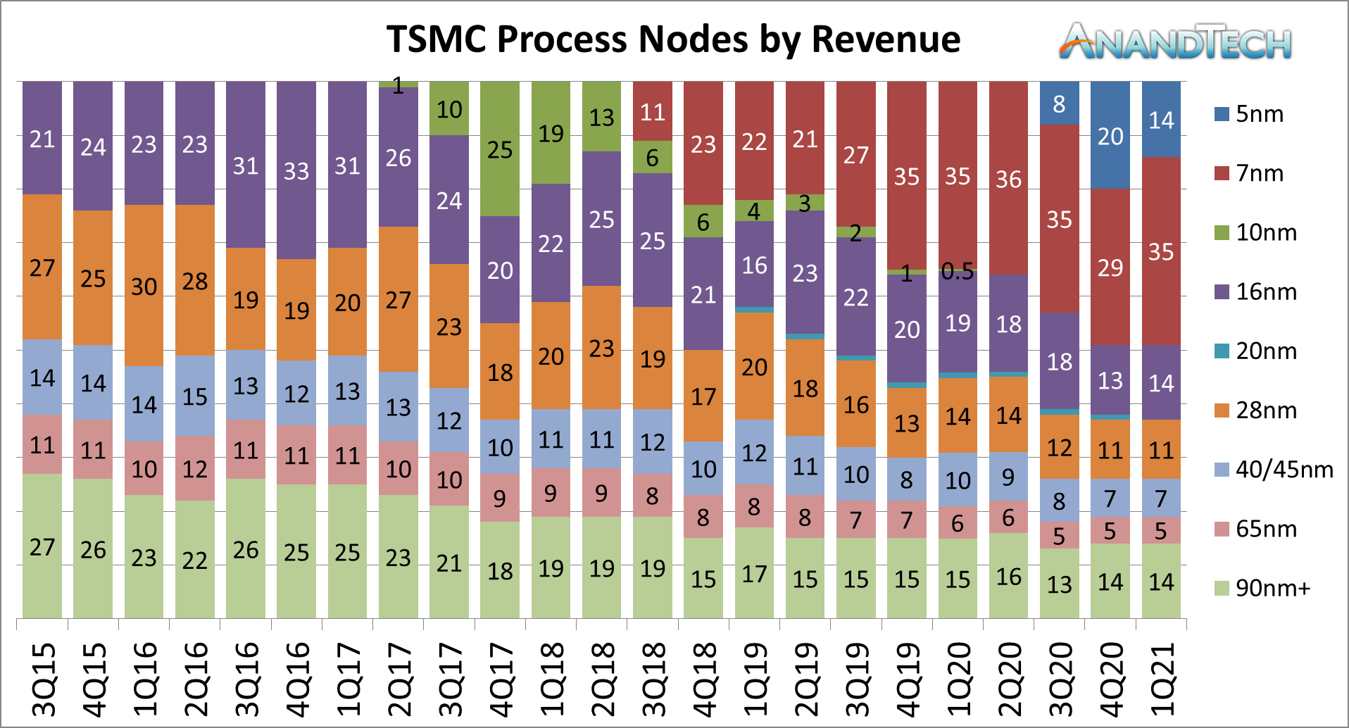
7nm accounts for 35% of all revenue, with 5nm now at 14%. This might seem odd, however TSMC has very few customers with 5nm designs, but plenty for 7nm, suggesting that TSMC is able to have customers bid against each other (along with increasing wafer output). For the last few quarters, reports about TSMC’s 7nm lead time for products, from order to production to shipment, have been extending due to the increased demand. Note that TSMC’s most advanced packaging technologies, such as CoWoS, are typically used in conjunction with 7nm or 16nm silicon, so those revenues are likely in those respective segments as well.
Recently TSMC has stated that it plans to spend $100B over the next three years to increase capacity leading-edge capacity, which includes the $25B-$28B it had already planned for 2021, with $12B of that going onto a factory in Arizona. To put that in perspective, TSMC’s Fab 15 which currently produces 12-inch wafers on 7nm, cost $9.3 billion in 2010, and has the capacity for ~100,000 wafer starts per month.
Revenue from 16nm is decreasing, now going below 15% for a couple of quarters, and showcasing that TSMC is making as much money from 16nm as it is from 5nm and 90nm+ older process nodes.
Also on this breakdown of process nodes, we can see that 20nm has bit the bullet, and now rounds to 0% of TSMC’s revenue. Both 20nm and 10nm are now listed at 0% as companies that produced hardware on these nodes are coming to the end of replacement life cycles for those products.
Demand for the older process nodes is still strong, with 28nm and above being 37% of the company revenue, which combined is more than 7nm revenue. Lots of fundamental electronics still require these process nodes, such as high voltage components, high thermal support/long life cycle hardening, or radio frequency silicon that is mature and low cost. Even TSMC’s interposer technology is manufactured on these process nodes, showcasing that the future is going to be a mix of old and new.
Also on TSMC’s disclosure is revenue by platform. The two major markets here are smartphone (45% by revenue) and high-performance computing (35% by revenue), which have consistently been about 80% of the total revenue for TSMC for over a year. The other 20% is taken up by IoT (9%), Automotive (4%), and others (7%).
Full details can be found on TSMC’s Investor Relations website.
From AnandTech’s perspective, we covered TSMC’s Tech Day 2020 disclosures in late August, covering the following topics:
- TSMC: We have 50% of All EUV Installations, 60% Wafer Capacity
- TSMC and Graphcore Prepare for AI Acceleration on 3nm
- Where are my GAA-FETs? TSMC to Stay with FinFET for 3nm
- 2023 Interposers: TSMC Hints at 3400mm2 + 12x HBM in one Package
- TSMC Expects 5nm to be 11% of 2020 Wafer Production (sub 16nm)
- TSMC’s Version of EMIB is ‘LSI’: Currently in Pre-Qualification
- TSMC Teases 12-High 3D Stacked Silicon: SoIC Goes Extreme
- TSMC Updates on Node Availability Beyond Logic: Analog, HV, Sensors, RF
- ‘Better Yield on 5nm than 7nm’: TSMC Update on Defect Rates for N5
- TSMC Launches New N12e Process: FinFET at 0.4V for IoT
- 3DFabric: The Home for TSMC’s 2.5D and 3D Stacking Roadmap


40 Comments
View All Comments
Zoolook - Tuesday, April 20, 2021 - link
Neither AMD nor Nvidia used 20 nm, they stayed on 28nm until they moved to 16nm, which led to 28nm being the node that holds the record for most generations of pc graphics in recent years. It was a cludge of a node with relatively small benefits and cost/performance increased compared to staying on 28nm.The Von Matrices - Friday, April 16, 2021 - link
TSMC 20nm was a dud with high leakage and minimal scaling over 28nm, so it makes sense for discontinuation. 20nm was TSMC's smallest process using planar transistors; TSMC "16nm" is just rebranded 20nm with FinFETs.TristanSDX - Friday, April 16, 2021 - link
shares at revenue, says nothing as price of wafer vary depending on processhanselltc - Monday, April 19, 2021 - link
Why is 10 so dead lolRSAUser - Tuesday, April 20, 2021 - link
Because it was finfet, those tools and fabs were repurposed for 7nm.hanselltc - Tuesday, April 20, 2021 - link
I seeZoolook - Tuesday, April 20, 2021 - link
I'd wish Anandtech would use the proper descriptions of wafer tech, the so called 12-inch wafers are actually 300mm or 11.8 inches.ET - Tuesday, April 20, 2021 - link
I don't understand the market division. 80% for HPC and smartphones would mean (for example) that 40nm and down are all in these segments. I can believe that there are phone chips being manufactured on older processes, but to this extent?Atom2 - Tuesday, April 27, 2021 - link
Something must have happened around 2016 at TMSC, because they were able to to go 16 to 10, 10 to 7, 7 to 5 in 1.5year intervals. Intel needed six years to make transition from 14 to 10. TMSC is moving at 4x the speed of Intel, when it comes to process nodes. Intel would need to improve its process delivery performance by nearly 10x to overtake TMSC in next 10 years.Sorcery - Wednesday, April 28, 2021 - link
I think it was TSMC's partnership and nurturing of ASML that paid off. TSMC is ASML's biggest customer. There is some comment on what ASML is doing here (absent the nurturing by TSMC) here https://www.fool.com/investing/2021/04/21/better-s...