AMD and Samsung's GPU Licensing Deal: A New Era of Collaboration?
by Ryan Smith & Andrei Frumusanu on June 7, 2019 7:00 PM EST
Back on Monday we saw the surprise announcement from AMD and Samsung revealing a multi-year strategic partnership in which Samsung will license AMD’s graphics IP. Since the announcement, we’ve been working to reach out to sources to try to dig a bit deeper into just what the deal entails. While it seems like AMD and Samsung are holding their most important cards close to their proverbial chest, we’ve managed to find some new high-level details of the deal, and how it looks like AMD and Samsung are setting up for a rather unique collaborative arrangement.
Perhaps the biggest outstanding question is just how the licensing arrangement works – what exactly has Samsung licensed? It’s also the trickiest question, and the one that our sources have been the least willing to talk about. So we're going to put a pin in that for the moment, so that we can talk about another few points first.
Samsung Goes “Next Gen” In 2022+ (or later)
Instead, let’s start with GPU architectures and the timing of the deal, since these factors are closely intertwined. We’ve known for some time now that Samsung has been working on their own GPU design, making it so far as to producing test chips on 10nm and 7nm. While we don’t have detailed information, it does look that things haven’t been progressing quite as fast as Samsung had hoped.
From all perspectives, it looks like this AMD/Samsung deal was only more recently finalized, and that the two companies are just at the start of their partnership. In particular, Samsung's VP of GPU development seems to have only a few days ago changed his employment status as no longer being with the company, which is one of a few indicators we're aware of that Samsung only recently changed strategies.
This also means that whatever Samsung started working on, it’s going to take some time to bring it to market. Even if this is a crash program – and to be clear, we don’t get that impression here – it will still take Samsung some time to integrate AMD’s GPU IP and tune it for SoC performance and power levels. That would seem to be a minimum of two years, if not longer, so we’re not expecting to see Radeon-powered Samsung SoCs any sooner than 2022.
The timing also points out that that this would be a future AMD GPU architecture that Samsung will be working with, rather than something that contemporary to AMD’s current products. While AMD is currently ramping up production of GPUs based on the Navi architecture, and these are going to hit the market in July, we have to keep in mind that these designs were probably locked in 2 years ago.
As such, for the 2022 product time frame, it means that Navi would already be four to five years old by the time Samsung’s first SoC ships. So, while our sources have confirmed that Samsung is using a GPU architecture on AMD’s public roadmap, it’s apparently not Navi.
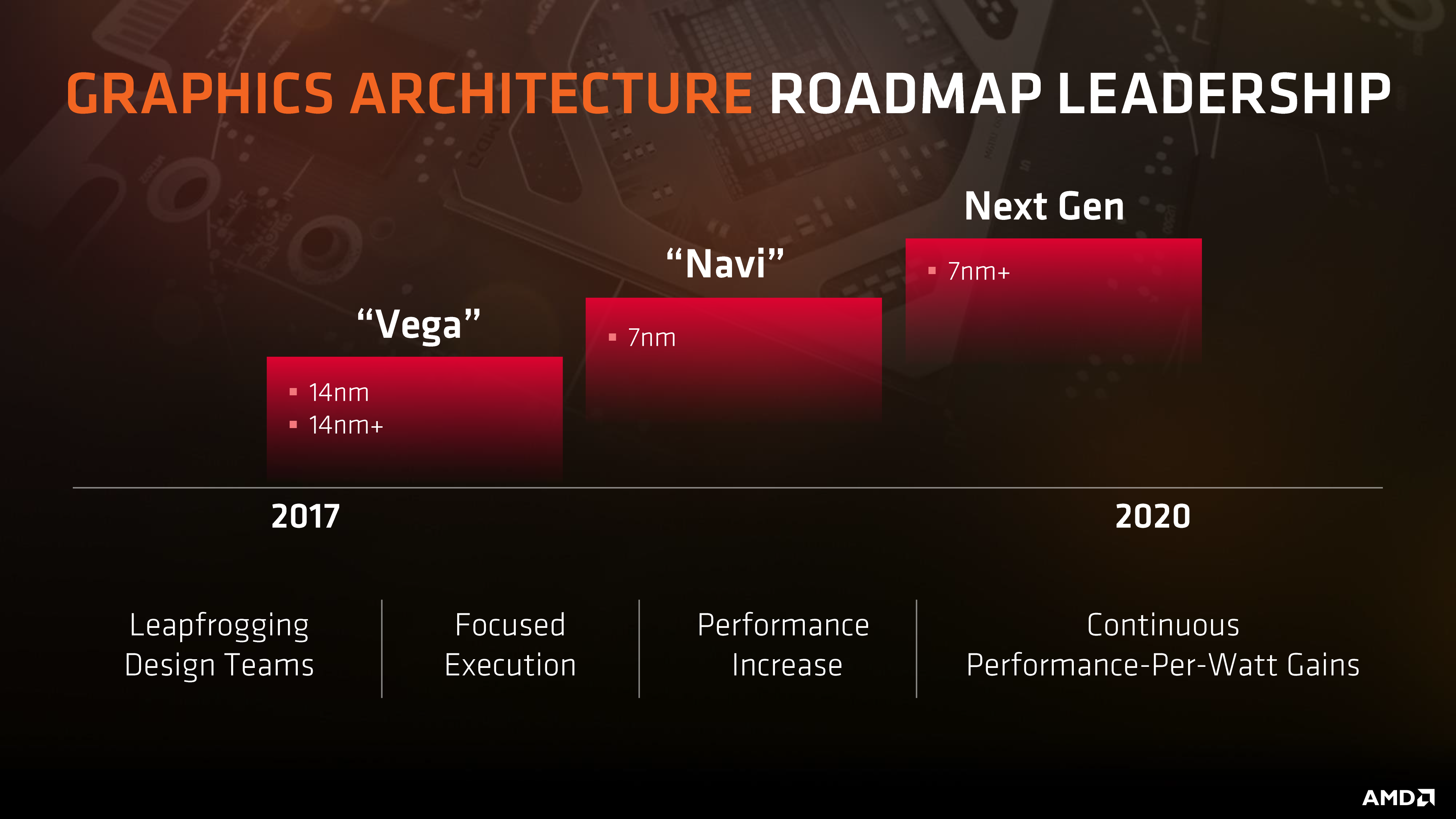
Thankfully, AMD’s GPU public roadmap is short and simple. There’s only one architecture on the roadmap after Navi, and that is the enigmatic “Next Gen” architecture. Essentially nothing is known about this architecture other than that its microarchitectures are being developed in a leapfrog style – so it’s the team not working on Navi – and that AMD is focused on continuing to improve their performance and power efficiency. Given what little we know about Navi (even though it’s launching next month) we won’t go into speculation about just what “Next Gen” entails, but regardless it’s going to be the basis of Samsung’s first generation of Radeon RDNA-derived GPUs.
Samsung Can’t Compete with AMD: Smartphones & Tablets Only
Shifting gears, another piece of information we’ve been able to confirm what the press release’s mention of “complementary products” means, and it’s pretty straightforward. In short, the AMD/Samsung deal is structured so that Samsung is only allowed to use AMD GPU IP in segments that AMD doesn’t compete in. In other words, AMD’s GPU tech can only be used in smartphone and tablet SoCs. For anything else, Samsung is either prohibited from using the tech, or at best, has to get AMD’s permission first.
This is an important distinction for both companies, because it ensures that licensing out their IP doesn’t undermine AMD, and it means that Samsung can’t use it to break into new markets. For example, Windows on ARM devices are off the table, as AMD already produces APUs for laptops, and that market is only going to grow for them over time. Similarly, AMD’s lucrative (if small) embedded devices business (think casino machines and the like) would be safe.
As for Samsung, this means that while the tech deal stands to greatly improve the company’s GPU capabilities, their reach will be limited. So for the rivalry between Samsung LSI and Qualcomm, for example, while Samsung will be able to better compete against Qualcomm on mobile chips, this isn’t going to turn Samsung into a top-to-bottom competitor for Qualcomm’s SoC business.
Without the ability to produce chips for Windows on ARM and other markets, Samsung will only be able to use AMD’s GPU IP to counter Qualcomm’s Adreno GPUs in the mobile market. Which is by no means small, but it’s not Qualcomm’s entire SoC business, particularly with the rising focus of dedicated ACPC SoCs such as the Snapdragon 8CX.
Architecture Licensing: Not Semi-Custom, Not A Traditional Architecture License, So Collaborative?
Last, but not least, we have the biggest question of them all: just what has Samsung licensed from AMD? The original announcement had explained that Samsung will be licensing “custom graphics IP based on the highly-scalable RDNA architecture”, however those are relatively broad terms as to what exactly is being licensed.
Unfortunately, this is the part that our sources have been the least willing to talk about. So, what follows from here is speculation. However, based on what we have heard – and more importantly, what we can rule out – it’s very much informed speculation, and we think we have a pretty good idea of just how Samsung’s licensing deal works.
When you look at AMD and Samsung from a high level, what you’ll find is that the two companies have rather different approaches to IP. AMD has embraced IP licensing, but primarily in the form of “semi-custom” work – such as the Xbox and Playstation APUs – where AMD essentially does development work for hire for another company. Meanwhile Samsung’s model as an IP consumer is broadly defined as preferring to take an architecture from an IP supplier and customizing it to fit their needs. So AMD has little experience licensing out an architecture, and Samsung isn’t really interested in licensing finished microarchitecture RTL from another company. Both companies want a finger in the pie, so to speak.
Consequently then, we believe we can safely rule out this deal being a traditional AMD semi-custom deal. When AMD inks semi-custom deals, they’ve never been couched in terms of licensing IP. Furthermore – and with no intended disrespect to AMD – AMD’s track record on energy efficiency GPU designs has been poor for the last half-decade or so. So having AMD design a SoC-class GPU on their own seems like a poor idea.
Does that mean that Samsung has licensed a complete GPU architecture to do what they want, ala an Arm CPU architecture license? At first glance this would seem to be the case; but the more we dig, the less likely it seems. We have serious doubts over whether AMD would be comfortable with such a thing – just handing over IP and letting Samsung turn it into whatever they want – not to mention the fact that Samsung doesn’t currently have any experience with AMD’s GPU IP.
Bearing in mind that Samsung’s own GPU efforts haven’t yet been fruitful, even after years of research & development, Samsung may not want to dive into the deep end of a new architecture all by themselves if they have the end-goal of actually productising the IP.
So what’s left then? Would you believe about 11 miles?
One of the interesting artifacts of how centralized the technology industry is, is that AMD and Samsung aren’t very far away. In fact they’re downright close. Samsung’s Austin, Texas SARC development office is only 11 miles from AMD’s headquarters, while their GPU-focused ACL team lies in San Jose, California, where AMD also has offices. So while the companies may officially be centred on opposite sides of the world, the reality is that their IP and silicon development efforts are a lot closer.
The more thought we put into it and the more research we do, the more that all signs are pointing towards the licensing deal not being semi-custom or a straight-up architecture license, but rather a collaborative deal. A kind of deal where AMD could give Samsung access to their IP, and then the two could work together and combine their strengths to produce a better, more appropriate GPU sooner. This would essentially bridge the gap between the two companies and their preferences for IP licensing – Samsung would still get to work with AMD’s IP and architecture, but they wouldn’t have to go it alone, and AMD wouldn’t be losing control of what’s happening to their architecture.
Besides bridging their respective styles, a collaborative deal would also (relatively) neatly resolve some of the technical issues at hand. Samsung would be putting forth a lot of engineering resources themselves, in particular being able to drive the kind of customization they’re looking for in a SoC GPU – incorporating the features that Samsung needs for this kind of a market. At the same time it also means that Samsung could apply their extensive expertise in power optimizations, which has been a weak spot for AMD. And yet Samsung wouldn’t have to come into this knowing every last minor detail of AMD’s architecture and how to change it, as AMD would be there to help them with that.
A collaborative deal would also make more sense than a pure architecture license as far as the development toolset and ecosystem goes. One point AMD was eager to mention in their joint press release is that “This strategic partnership will extend the reach of our high-performance Radeon graphics into the mobile market, significantly expanding the Radeon user base and development ecosystem”. If Samsung were allowed to change AMD’s IP at will – to deviate from the Radeon design as they see fit – then the architectures would diverge and Samsung’s SoCs would risk becoming increasingly un-Radeon. Instead, AMD seems rather confident that they’ll be able to count software developers programming against the Samsung SoCs as part of the Radeon ecosystem, which strongly implies that AMD knows that whatever Samsung implements, it won’t be too different from AMD’s own designs.
Assuming we’re correct, then what Samsung would be able to achieve is to take full advantage of AMD’s current leading GPU architecture, while still having the freedom to adapt and change it based on their needs and create a microarchitecture that fits the mobile space. Most importantly for Samsung and in contrast to third-party IP providers such as Arm or Imagination, this deal would enable them to achieve (micro-)architecture-implementation co-optimization. This means that based on feedback of their physical implementation work when integrating an IP into a SoC design, Samsung could go back and change the architecture/micro-architecture in order to achieve better implementation results, thus improving on power, performance and area. Importantly, this currently isn’t possible with, say Mali designs, as a licensee isn’t able, nor is he allowed to alter the IP they receive from Arm.
Meanwhile a collaboration benefits AMD as well. Such a deal would essentially open up a new revenue stream in the mobile market, but without the company having to actually go ahead and create a full new division and as extensive support framework as a full-blown IP vendor. Nor, for that matter, would they have to do any physical implementation work or create any dedicated mobile microarchitectures. And since the deal is structured to ensure Samsung’s products only complement AMD’s products – all the while Samsung is paying AMD – a collaboration would only benefit AMD.
But, even if our assumption is right here, the one question even the crystal ball can’t answer is what kind of role Samsung’s existing IP will play in this new partnership. Even though Samsung’s SGPU project wasn’t productised, Samsung has still developed a pool of talent and IP that they can apply to future projects. It seems likely that significant resources in Samsung’s GPU design-centers both in Austin and San Jose would be needed (if not already) to be shifted to work on the new AMD project. Something that’s equally ambiguous – but could have a big impact on how the deal works – is whether Samsung can use any of their existing IP with the new project, or for that matter who ends up owning any co-developed IP by the partnership. And there’s the big open question of whether AMD can use any IP improvements that were co-developed into their own products, or if they’ll be treated as a work-for-hire and stay with Samsung.
In the end, AMD’s licensing deal with Samsung looks to be something unlike we’ve seen in the industry. With a very large emphasis on long term strategic partnering – and, if we’re right, a novel co-development structure – which in general it looks like an absolute win-win for both companies.


94 Comments
View All Comments
AshlayW - Friday, June 7, 2019 - link
To be fair on AMD and GPU energy efficiency: the desktop Radeon cards are by no means a fair benchmark of GCN's efficiency, especially if you scale it down to a mobile SoC. What these cards' comparatively poor performance per watt (versus Nvidia for example) demonstrates, is poor performance per watt *scaling* at high performance levels. Ugh did I word this correctly?I mean that, those cards are pushes so far out of the architecture efficiency curve, because they didn't scale up to that performance efficiently. I would point out that at much lower performance levels and power optimised, GCN cards can be just as efficient as Pascal and potentially Turing: just at a much lower overall performance tier.
The mobile Ryzen APUs can demonstrate how efficient GCN can be.
webdoctors - Friday, June 7, 2019 - link
But can GCN scale down to the tablet/phone sub 5W envelope that well? Wouldn't Samsung partnering with Imagination make way more sense?Alexvrb - Friday, June 7, 2019 - link
I think they should have BOUGHT Imagination Technologies. They have some impressive designs, and with Samsung's cash they could do great things again.But yes, GCN can scale down and becomes far more efficient at lower power envelopes. You've already got laptop APUs on 14nm (and soon 12nm Picasso) that can TDP-down to 12W, and they include 4 full Zen cores and 10 CUs of last-gen GCN. That's just with old tech... take the next-gen GPU designs, customize them, and pair them with power-sipping ARM cores and more power efficient process tech.
niva - Monday, June 10, 2019 - link
They might very well buy Imagination Tech anyways. The way Samsung goes about business is to wage battle on multiple fronts and later determine which was the valid path forward. It's one of the biggest reasons why they're murdering the competition and probably approaching world-wide monopolistic scale in the tech world.StevoLincolnite - Friday, June 7, 2019 - link
There is a massive divide between 200w and 2w of power though.Yes, GCN can scale down in powerlevels really well, Vega 64 for instance was actually extremely efficient when you dropped the clocks and voltages... But instead AMD blew those two aspects out to get as much performance as possible to remain semi-competitive in the mid-high-end.
levizx - Monday, June 10, 2019 - link
If you consider existing Mobile Ryzen APU@15W, which already delivers up to 4 times the performance of Snapdragon 82x@5W, on the same process node, it's not that hard to believe even without substantial modification, they can deliver something at least equal to Adreno by the end of the year, just in time for 2021 Exynos.yannigr2 - Saturday, June 8, 2019 - link
AMD is far behind in efficiency, in both CPUs and GPUs. While APUs can be considered efficient, based on their TDPs, they can't offer the battery life that Intel processors can offer. That's why AMD is pushing in manufacturing by rushing to adopt 7nm.Dragonstongue - Saturday, June 8, 2019 - link
They are NOT AT ALL.for GPU depending on the specific generation, they are "just as good" as the other ( Nvidia ) and more often than not it was the Radeons that used less power / ran cooler / gave a better final end result (image quality or various other features) that is FACT.
HOWEVER, the generations that Nv was ahead in this regard, often were noticeably so, CPU wise.....Sorry to burst bubble, but Intel and AMD for the most part use the SAME or roughly the same wattage "over time" and truth be tole it is AMD actually with CPU and GPU that are more oft than not actually giving a very close to 100% true rating on their TDP/Board power etc without relying on fancy BS to achieve such.
in other words, Radeons (at least for the most part) are like junk yard Mac wreckers, sure they are louder, they sometimes belch some cobwebs, but darn it, they get any task done you need to do, and if you really want, take that wonking engine and put into a strip down race body and she just flies.
Nv has over 7 going on to 8 generations cut things away, added "dual" compute (or however want to call) to "trick" apps etc into using it like it is the full fat version when it is not, so they need fancy other chips.circuits to allow this, so the modern Nv is more like a Ferrari with all the fancy gauges that temperatures, heatsinks etc are as "cheap as can be, but quick acting" so instead of beefing up things such as better solder, better VRM and the like Intel and Nvidia whom you likely reference have cut things away, went to lower quality sub components (i.e paste instead of solder, solder instead of eutectic, 85/95 sometime 105c spec capacitor for VRM instead of at least 105/125 or 115/125c ...
So, while in aspect AMD did not do all that well below the 15w level, neither did Intel vs smartphone others and Nv is not the "golden child" folks keep pimping them up to be, they both ( Intel - Nv) do and still do A LOT of crap to mainly trick folks into continuing to use them regardless of what they are doing to make it so, as well, many folk sare BLIND BLIND BLIND to the point where their brand loyalty is the only thing that makes an iota of sense to their peanut of a brain.
Depending on product generation as well as how is used etc, Intel was "slightly" (last 20mins more for a bit more performance in a laptop as an example) but, at the same time the Radeons and AMD CPU, MOST PEOPLE who use them side by side to competing they all generally walk away "it feels the same, but I can actually have far more tabs open in my browser and it does not hitch as well I can leave system running for days-weeks-months and not really have to reboot fully ever with AMD/Radeon but with Intel/Nvidia I had to do a full shutdown once every 2 weeks like clock work or performance would just tank like crazy.....
I not trust numbers any of the "big whales" put out, as when a chip with a 105w TDP label is able to and consistently blows past this number (Intel 7-8-9 generations most recent) but yet the AMD ones you "claim" are SO FAR BEHIND rarely, truthfully rise above to much beyond 10% or so (which is spec to about 15% +/- rating not 30%+ BS STOCK...........
Phynaz - Saturday, June 8, 2019 - link
AMD fanboys are weirdMamiyaOtaru - Saturday, June 8, 2019 - link
why are you even bothering. Their new CPUs look to have caught up to Intel efficiency wise, but that'll be the first time since Conroe and everyone knows it. And nVidia? They've been lagging them on efficiency since Maxwell. https://www.techpowerup.com/reviews/EVGA/GTX_1650_... FFS. How do you look at that, and with a straight face vomit out some BS about them being toe to toe.The best I can say for your post was that it was so long I couldn't be bothered to read the whole thing so I probably missed a bunch more dumb stuff