AMD Shows Off Dual-GPU Fiji Card At PC Gaming Show
by Ryan Smith on June 17, 2015 8:00 AM EST
Briefly announced and discussed during AMD’s 2015 GPU product presentation yesterday morning was AMD’s forthcoming dual Fiji video card. The near-obligatory counterpart to the just-announced Radeon R9 Fury X, the unnamed dual-GPU card will be taking things one step further with a pair of Fiji GPUs on a single card.
Meanwhile as part of yesterday evening’s AMD-sponsored PC Gaming Show, CEO Dr. Lisa Su took the stage for a few minutes to show off AMD’s recently announced Fury products. And at the end this included the first public showcase of the still in development dual-GPU card.
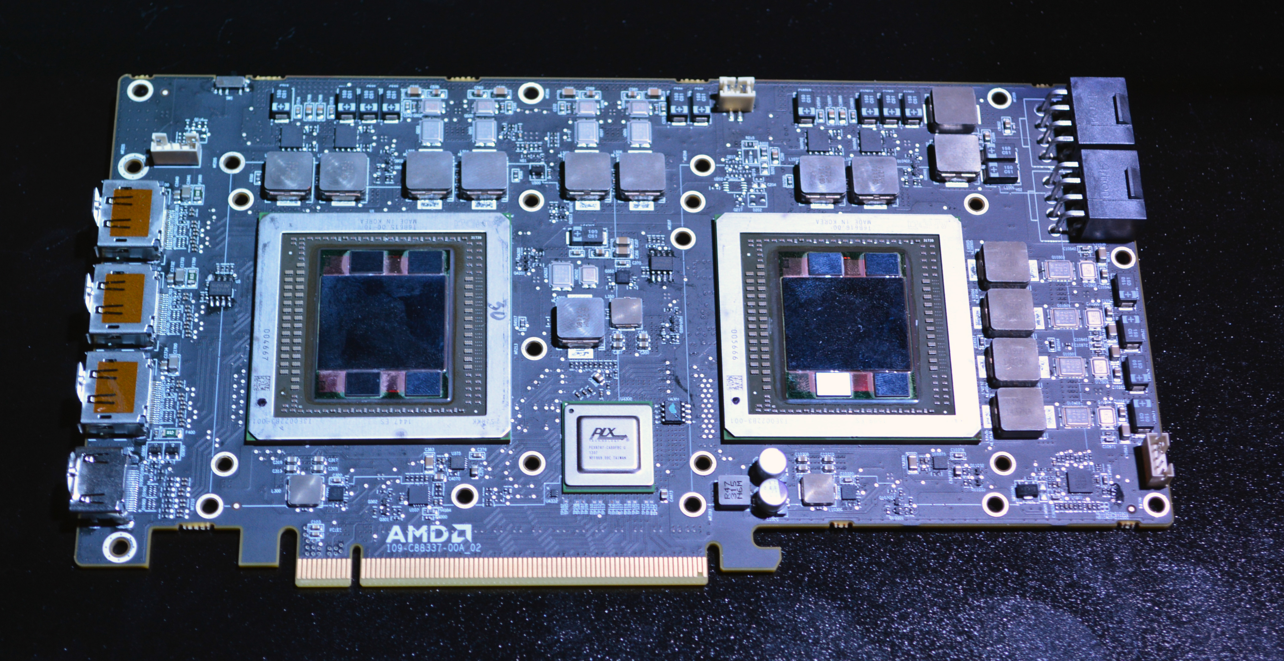
There’s not too much to say right now since we don’t know its specifications, but of course for the moment AMD is focusing on size. With 4GB of VRAM for each GPU on-package via HBM technology, AMD has been able to design a dual-GPU card that’s shorter and simpler than their previous dual-GPU cards like the R9 295X2 and HD 7990, saving space that would have otherwise been occupied by GDDR5 memory modules and the associated VRMs.
Meanwhile on the card we can see that it uses a PLX 8747 to provide PCIe switching between the two GPUs and the shared PCIe bus. And on the power delivery side the card uses a pair of 8-pin PCIe power sockets. At this time no further details are being released, so we’ll have to see what AMD is up to later on once they’re ready to reveal more about the video card.


133 Comments
View All Comments
TomWomack - Wednesday, June 17, 2015 - link
Why are there only four HBM stacks? It looks as if you could fit three down each side of that ludicrously big GPU die without enlarging the even-bigger silicon imposer.lilmoe - Wednesday, June 17, 2015 - link
Give it more time to mature. Fitting "only" 4 stacked modules isn't as easy as it seams.Mark_gb - Wednesday, June 17, 2015 - link
This is the first time any video card company has worked with HBM. They were putting the pieces into place as much as 2 years ago. And trying to figure out what they could do today. You can almost bet that they thought they would be doing at least 16nm by now, if not 14nm. And as we all know, both AMD and Nvidia have been stuck on 28nm.HBM will move to smaller nodes, stack higher, run at a faster speed, gain DDR technology, and all of that in a relative short period of time. And they should have enough confidence by next year to start using more HBM stacks with a GPU. Everything new always starts big and slow... and shrinks quickly as engineers understand it more, and become more comfortable with the product.
MrSpadge - Wednesday, June 17, 2015 - link
Plus:- they don't need more bandwidth than the 0.5 TB/s they already get now.
- and the chip is already so large at 596 mm², with 600 mm² being the current practical limit, that there was no space left to fit even one more of the comparably small HMB controllers
Kevin G - Wednesday, June 17, 2015 - link
Largest commercial die produced was the Tukwilia Itanium at an impressive 699 mm^2. Theoretical limit for how large a die can be is between 700 and 800 mm^2 during that era.If foundries ever move to 450 mm wafer sizes, producing such large chips will become far more feasible. However with interposers I would predict a reversing of that trend to smaller dies. Far easier to get good yields on two smaller dies than one larger unit. It makes sense from both a performance and cost perspective for designs using an interposer for HBM anyway.
tcube - Thursday, June 18, 2015 - link
Yeah! I would love 2 fiji dies on an interposer with a 4x HT(4.0?) link between the two, should make them work as one single gpu... imagine putting multiple smaller chips all interlinked with ht links, say use 1 link/chip and use smaller chips(1k sp's each) and a larger interposer. Would make the package quite complex but you should get much better scaling then with the cfx bullKevin G - Thursday, June 18, 2015 - link
It wouldn't even be HyperTransport, it'd be the native internal bus used on-die. Not need to use a topology like HT that was designed to work between sockets.tcube - Thursday, June 18, 2015 - link
Where did you read that fiji has a 596mm^2 diesize?(I knew something along the lines of 550-568) Btw Titanx has a diesize of 603^mmKevin G - Wednesday, June 17, 2015 - link
A bit of a nitpick but HBM already uses DDR bus. Most places are reporting a 1 Ghz clock speed but that's the effective rate. The real clock speed is a meager 500 Mhz.HBM2 is due next year and will bring both capacity and bandwidth increases on a per stack basis. As mentioned, there is room for more stacks if need be as well.
Though I'm of the mindset that instead of increasing die size and number of HBM stacks per die to astronomical levels, AMD will return to a small die strategy and simply use an interposer for in-package Crossfire. Bandwidth between dies shouldn't be an issue and latencies between units would be similar if the chip was monolithic. Say four GPU dies + eight HBM stacks for the high end product, two GPU + four HBM stacks for a midrange product and a single GPU die + two HBM stacks for the low end. Their SoC efforts could also benefit by having a dedicated CPU die and simply re-use this GPU die to complete the design. Rinse and repeat for the proper mixture of CPU cores and GPU assist. AMD would have a full product line up using only two actual logic dies plus a range of interposers. That would greatly simplify development, something AMD needs to be focused upon.
K_Space - Wednesday, June 17, 2015 - link
Will Pascal launch with HBM2 then?