AMD Dives Deep On High Bandwidth Memory - What Will HBM Bring AMD?
by Ryan Smith on May 19, 2015 8:40 AM EST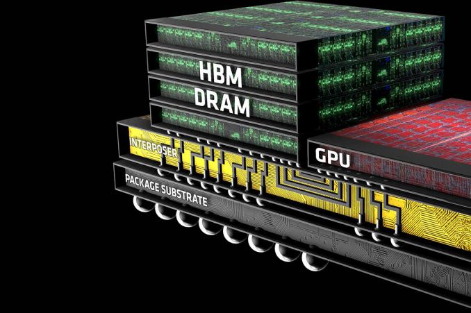
Though it didn’t garner much attention at the time, in 2011 AMD and memory manufacturer Hynix (now SK Hynix) publicly announced plans to work together on the development and deployment of a next generation memory standard: High Bandwidth Memory (HBM). Essentially pitched as the successor to GDDR, HBM would implement some very significant changes in the working of memory in order to further improve memory bandwidth and turn back the dial on memory power consumption.
AMD (and graphics predecessor ATI) for their part have in the last decade been on the cutting edge of adopting new memory technologies in the graphics space, being the first to deploy products based on the last 2 graphics DDR standards, GDDR4, and GDDR5. Consequently, AMD and Hynix’s announcement, though not a big deal at the time, was a logical extension of AMD’s past behavior in continuing to explore new memory technologies for future products. Assuming everything were to go well for the AMD and Hynix coalition – something that was likely, but not necessarily a given – in a few years the two companies would be able to bring the technology to market.
AMD Financial Analyst Day 2015
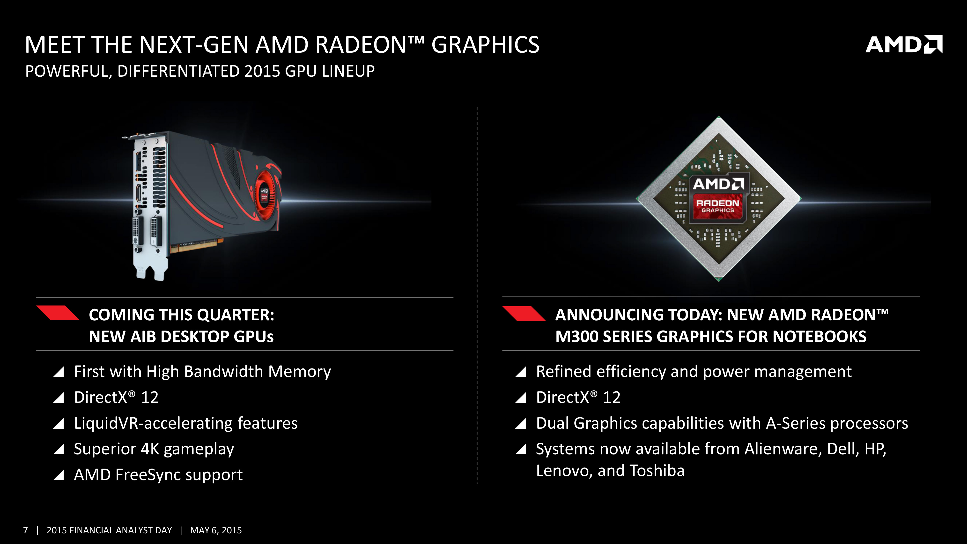
It’s now 4 years later, and successful experimentation has given way to productization. Earlier this month at AMD’s 2015 Financial Analyst day, the company announced that they would be releasing their first HBM-equipped GPU – the world’s first HBM-equipped GPU, in fact – to the retail market this quarter. Since then there have been a number of questions of just what AMD intends to do with HBM and just what it means for their products (is it as big of a deal as it seems?), and while AMD is not yet ready to reveal the details of their forthcoming HBM-equipped GPU, the company is looking to hit the ground running on HBM in order to explain what the technology is and what it can do for their products ahead of the GPU launch later that quarter.
To date there have been a number of presentations released on HBM, including by memory manufactures, the JEDEC groups responsible for shaping HBM, AMD, and even NVIDIA. So although the first HBM products have yet to hit retail shelves, the underpinnings of HBM are well understood, at least inside of engineering circles. In fact it’s the fact that HBM is really only well understood within those technical circles that’s driving AMD’s latest disclosure today. AMD sees HBM as a significant competitive advantage over the next year, and with existing HBM presentations having been geared towards engineers, academia, and investors, AMD is looking to take the next step and reach out to end-users about HBM technology.
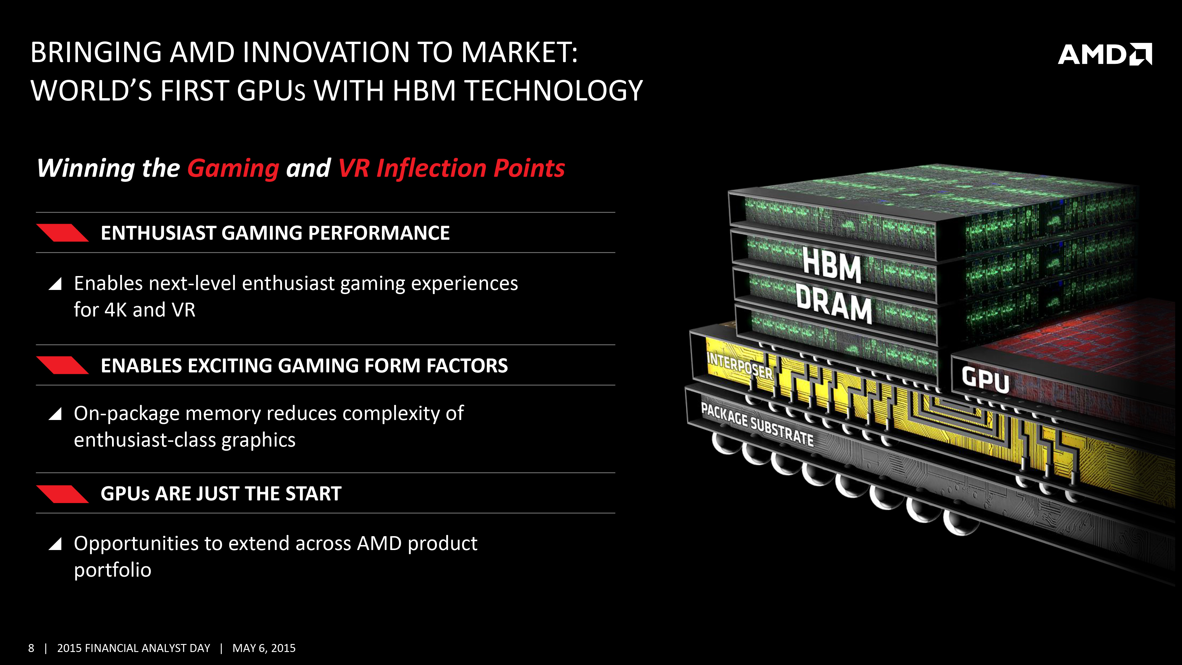
This brings us to the topic of today’s article: AMD’s deep dive disclosure on High Bandwidth Memory. Looking to set the stage ahead of their next GPU launch, AMD is reaching out to technical and gaming press to get the word out about HBM and what it means for AMD’s products. Ideally for AMD, an early disclosure on HBM can help to drum up interest in their forthcoming GPU before it launches later this quarter, but if nothing else it can help answer some burning questions about what to expect ahead of the launch. So with that in mind, let’s dive in.
I'd also like to throw out a quick thank you to AMD Product CTO and Corporate Fellow Joe Macri, who fielded far too many questions about HBM.


163 Comments
View All Comments
akamateau - Thursday, May 28, 2015 - link
You miss the whole point.DX12 solves Witcher.
HBM was designed to manage the high volume of drawcalls that DX12 enables.
ALL GPU's were crippled with DX11. DX11 is DEAD.
You can't render an object until you draw it. Dx11 does not support multicore or multithreaded cpu processing of graphics, DX12 does.
With DX12 ALL CPU cores feed the GPU.
akamateau - Monday, June 8, 2015 - link
If AMD can put 4-8 gigs of HBM on a GPU then they can do the same with CPU's as well as APU's. All of the Patents that I am showing below reference 3d statcked memoryIn fact one interesting quote from the patents listed below is this:
"Packaging chips in closer proximity not only improves performance, but can also reduce the energy expended when communicating between the processor and memory. It would be desirable to utilize the large amount of "empty" silicon that is available in an interposer."
AMD has plans to fill that empty silicon with much more memory.
The point: REPLACE SYSTEM DYNAMIC RAM WITH ON-DIE HBM 2 OR 3!
Eliminating the electrical path distance to a few millimeters from 4-8 centimeters would be worth a couple of clocks of latency. If AMD is building HBM and HBM 2 then they are also building HBM 3 or more!
Imagine what 64gb of HBM could do for a massive server die such as Zen? The energy savings alone would be worth it never mind the hugely reduced motherboard size, eliminating sockets and RAM packaging. The increased amount of CPU's/blade or mobo also reduces costs as servers can become much more dense.
Most folks now only run 4-8 gigs in their laptops or desktops. Eliminating DRAM and replacing it with HBM is a huge energy and mechanical savings as well as a staggering performance jump and it destroys DDR5. That process will be very mature in a year and costs will drop. Right now the retail cost of DRAM per GB is about $10. Subtract packaging and channel costs and that drops to $5 or less. Adding 4-8 GB of HBM has a very cheap material cost, likely the main expense is the process, testing and yields. Balance that against the energy savings MOBO real estate savings and HBM replacing system DRAM becomes even more likely without the massive leap in performance as an added benefit.
The physical cost savings is quite likely equivalent to the added process cost. Since Fiji will likely be released at a very competitive price point.
AMD is planning on replacing system DRAM memory with stacked HBM. Here are the Patents. They are all published last year and this year with the same inventor; Gabriel H. Loh and the assignee is of course AMD.
Stacked memory device with metadata management
WO 2014025676 A1
"Memory bandwidth and latency are significant performance bottlenecks in many processing systems. These performance factors may be improved to a degree through the use of stacked, or three-dimensional (3D), memory, which provides increased bandwidth and reduced intra-device latency through the use of through-silicon vias (TSVs) to interconnect multiple stacked layers of memory. However, system memory and other large-scale memory typically are implemented as separate from the other components of the system. A system implementing 3D stacked memory therefore can continue to be bandwidth-limited due to the bandwidth of the interconnect connecting the 3D stacked memory to the other components and latency-limited due to the propagation delay of the signaling traversing the relatively-long interconnect and the handshaking process needed to conduct such signaling. The inter-device bandwidth and inter-device latency have a particular impact on processing efficiency and power consumption of the system when a performed task requires multiple accesses to the 3D stacked memory as each access requires a back-and-forth communication between the 3D stacked memory and thus the inter-device bandwidth and latency penalties are incurred twice for each access."
Interposer having embedded memory controller circuitry
US 20140089609 A1
" For high-performance computing systems, it is desirable for the processor and memory modules to be located within close proximity for faster communication (high bandwidth). Packaging chips in closer proximity not only improves performance, but can also reduce the energy expended when communicating between the processor and memory. It would be desirable to utilize the large amount of "empty" silicon that is available in an interposer. "
Die-stacked memory device with reconfigurable logic
US 8922243 B2
"Memory system performance enhancements conventionally are implemented in hard-coded silicon in system components separate from the memory, such as in processor dies and chipset dies. This hard-coded approach limits system flexibility as the implementation of additional or different memory performance features requires redesigning the logic, which design costs and production costs, as well as limits the broad mass-market appeal of the resulting component. Some system designers attempt to introduce flexibility into processing systems by incorporating a separate reconfigurable chip (e.g., a commercially-available FPGA) in the system design. However, this approach increases the cost, complexity, and size of the system as the system-level design must accommodate for the additional chip. Moreover, this approach relies on the board-level or system-level links to the memory, and thus the separate reconfigurable chip's access to the memory may be limited by the bandwidth available on these links."
Hybrid cache
US 20140181387 A1
"Die-stacking technology enables multiple layers of Dynamic Random Access Memory (DRAM) to be integrated with single or multicore processors. Die-stacking technologies provide a way to tightly integrate multiple disparate silicon die with high-bandwidth, low-latency interconnects. The implementation could involve vertical stacking as illustrated in FIG. 1A, in which a plurality of DRAM layers 100 are stacked above a multicore processor 102. Alternately, as illustrated in FIG. 1B, a horizontal stacking of the DRAM 100 and the processor 102 can be achieved on an interposer 104. In either case the processor 102 (or each core thereof) is provided with a high bandwidth, low-latency path to the stacked memory 100.
Computer systems typically include a processing unit, a main memory and one or more cache memories. A cache memory is a high-speed memory that acts as a buffer between the processor and the main memory. Although smaller than the main memory, the cache memory typically has appreciably faster access time than the main memory. Memory subsystem performance can be increased by storing the most commonly used data in smaller but faster cache memories."
Partitionable data bus
US 20150026511 A1
"Die-stacked memory devices can be combined with one or more processing units (e.g., Central Processing Units (CPUs), Graphics Processing Units (GPUs), and Accelerated Processing Units (APUs)) in the same electronics package. A characteristic of this type of package is that it can include, for example, over 1000 data connections (e.g., pins) between the one or more processing units and the die-stacked memory device. This high number of data connections is significantly greater than data connections associated with off-chip memory devices, which typically have 32 or 64 data connections."
Non-uniform memory-aware cache management
US 20120311269 A1
"Computer systems may include different instances and/or kinds of main memory storage with different performance characteristics. For example, a given microprocessor may be able to access memory that is integrated directly on top of the processor (e.g., 3D stacked memory integration), interposer-based integrated memory, multi-chip module (MCM) memory, conventional main memory on a motherboard, and/or other types of memory. In different systems, such system memories may be connected directly to a processing chip, associated with other chips in a multi-socket system, and/or coupled to the processor in other configurations.
Because different memories may be implemented with different technologies and/or in different places in the system, a given processor may experience different performance characteristics (e.g., latency, bandwidth, power consumption, etc.) when accessing different memories. For example, a processor may be able to access a portion of memory that is integrated onto that processor using stacked dynamic random access memory (DRAM) technology with less latency and/or more bandwidth than it may a different portion of memory that is located off-chip (e.g., on the motherboard). As used herein, a performance characteristic refers to any observable performance measure of executing a memory access operation."
“NoC Architectures for Silicon Interposer Systems Why pay for more wires when you can get them (from your interposer) for free?” Natalie Enright Jerger, Ajaykumar Kannan, Zimo Li Edward S. Rogers Department of Electrical and Computer Engineering University of Toronto Gabriel H. Loh AMD Research Advanced Micro Devices, Inc”
http://www.eecg.toronto.edu/~enright/micro14-inter...
“3D-Stacked Memory Architectures for Multi-Core Processors” Gabriel H. Loh Georgia Institute of Technology College of Computing”
http://ag-rs-www.informatik.uni-kl.de/publications...
“Efficiently Enabling Conventional Block Sizes for Very Large Die-stacked DRAM Caches” Gabriel H. Loh⋆ Mark D. Hill†⋆ ⋆ AMD Research † Department of Computer Sciences Advanced Micro Devices, Inc. University of Wisconsin – Madison”
http://research.cs.wisc.edu/multifacet/papers/micr...
All of this adds up to HBM being placed on-die as a replacement of or maybe supplement to system memory. But why have system DRAM if you can build much wider bandwidth memory closer to the CPU on-die? Unless of course you build socketed HBM DRAM and a completely new system memory bus to feed it.
Replacing system DRAM memory with on-die HBM has the same benefits for the performance and energy demand of the system as it has for GPU's. Also it makes for smaller motherboards, no memory sockets and no memory packaging.
Of course this is all speculation. But it also makes sense.
amilayajr - Tuesday, June 16, 2015 - link
With HBM in mind. Does AMD holds the patent for this? Is Nvidia just going to use HBM for free? Any one care to elaborate ? Because if Nvidia gets to use it for free then that's really funny for AMD side considering they are the one who research it and developed it. Am I making sense?