TSMC Unveils N2 Process Node: Nanosheet-based GAAFETs Bring Significant Benefits In 2025
by Anton Shilov on June 16, 2022 3:45 PM EST- Posted in
- Semiconductors
- TSMC
- 2nm
- N2
At its 2022 Technology Symposium, TSMC formally unveiled its N2 (2 nm class) fabrication technology, which is slated to go into production some time in 2025 and will be TSMC's first node to use their nanosheet-based gate-all-around field-effect transistors (GAAFETs). The new node will enable chip designers to significantly reduce the power consumption of their products, but the speed and transistor density improvements seem considerably less tangible.
TSMC's N2 is a brand-new platform that extensively uses EUV lithography and introduces GAAFETs (which TSMC calls nanosheet transistors) as well as backside power delivery. The new gate-all-around transistor structure promises well-published advantages, such as greatly reduced leakage current (now that the gates are around all four sides of the channel) as well as ability to adjust channel width to increase performance or lower power consumption. As for the backside power rail, it is generally designed to enable better power delivery to transistors, offering a solution to the problem of increasing resistances in the back-end-of-line (BEOL). The new power delivery is slated to increase transistor performance and lower power consumption.
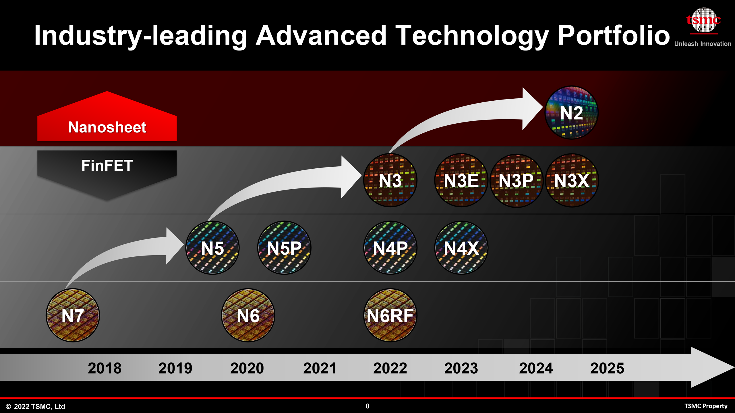
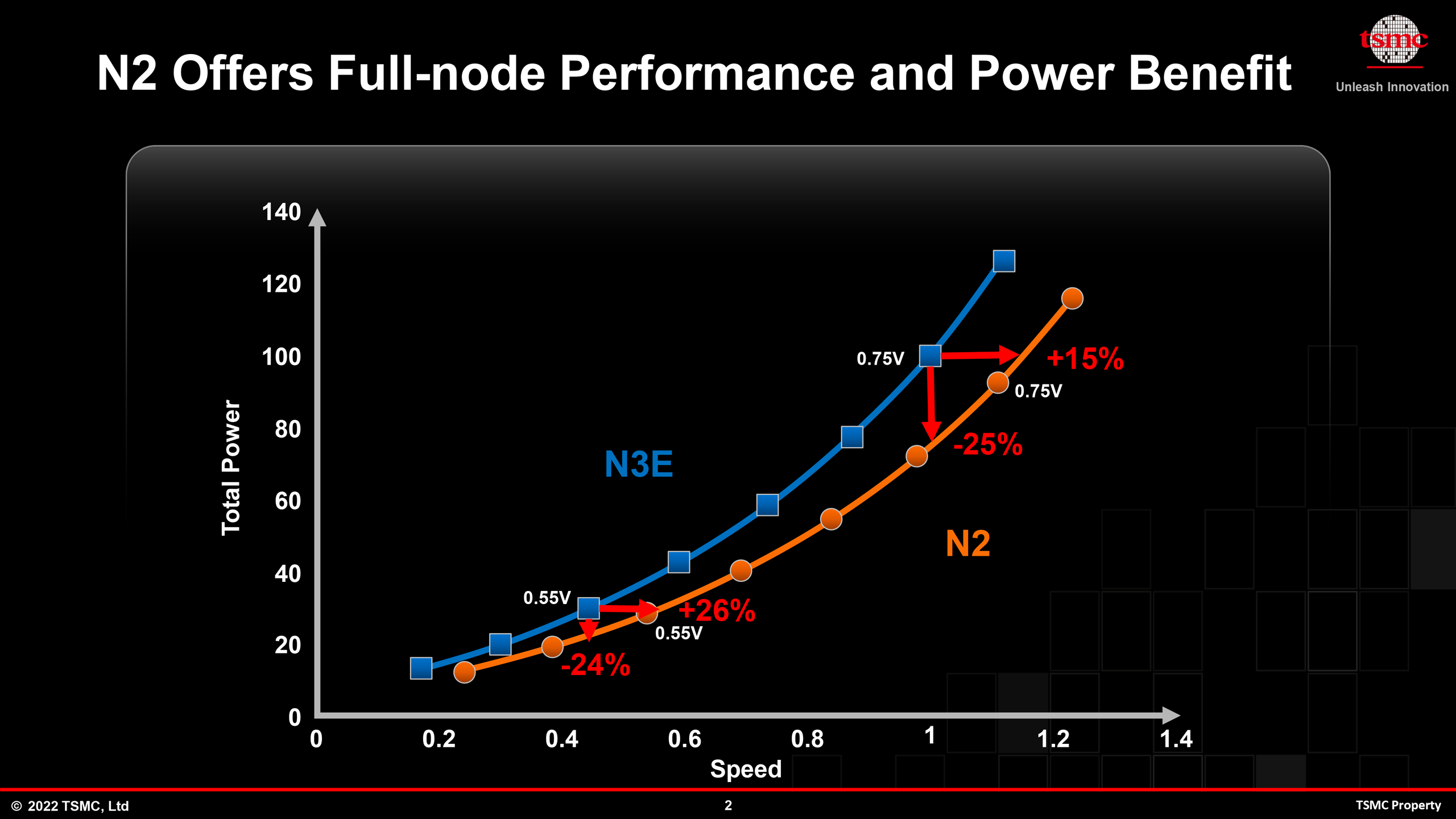
From feature set standpoint, TSMC's N2 looks like a very promising technology. As for actual numbers, TSMC promises that N2 will allow chip designers to increase performance by 10% to 15% at the same power and transistor count, or reduce power consumption at the same frequency and complexity by 25% ~ 30%, all the while increasing chip density by over 1.1-fold when compared to N3E node.
| Advertised PPA Improvements of New Process Technologies Data announced during conference calls, events, press briefings and press releases |
|||||
| TSMC | |||||
| N5 vs N7 |
N3 vs N5 |
N3E vs N5 |
N2 vs N3E |
||
| Power | -30% | -25-30% | -34% | -25-30% | |
| Performance | +15% | +10-15% | +18% | +10-15% | |
| Chip Density* | ? | ? | ~1.3X | >1.1X | |
| Volume Manufacturing |
Q2 2022 | H2 2022 | Q2/Q3 2023 | H2 2025 | |
*Chip density published by TSMC reflects 'mixed' chip density consisting of 50% logic, 30% SRAM, and 20% analog.
Versus N3E, the performance improvements and power reductions enabled by TSMC's N2 node are in line with what the foundry's new nodes typically bring in. But the so-called chip density improvements (which should reflect transistor density gains) are just a little over 10%, which is not particularly inspiring, especially considering that N3E already offers a slightly lower transistor density when compared to vanilla N3. Keeping in mind that SRAM and analog circuits barely scale these days, mediocre improvements in transistor density of actual chips should probably be expected these days. However, a chip density improvement of 10% in about three years is certainly not great news for GPUs and other chips that live or die based on rapidly increasing their transistor counts.
Bearing in mind that by the time TSMC's N2 enters production the company will also have the density-optimized N3S node, it would appear that the foundry will have two process technologies based on different types of transistors yet offering very similar transistor densities, something that has never happened before.
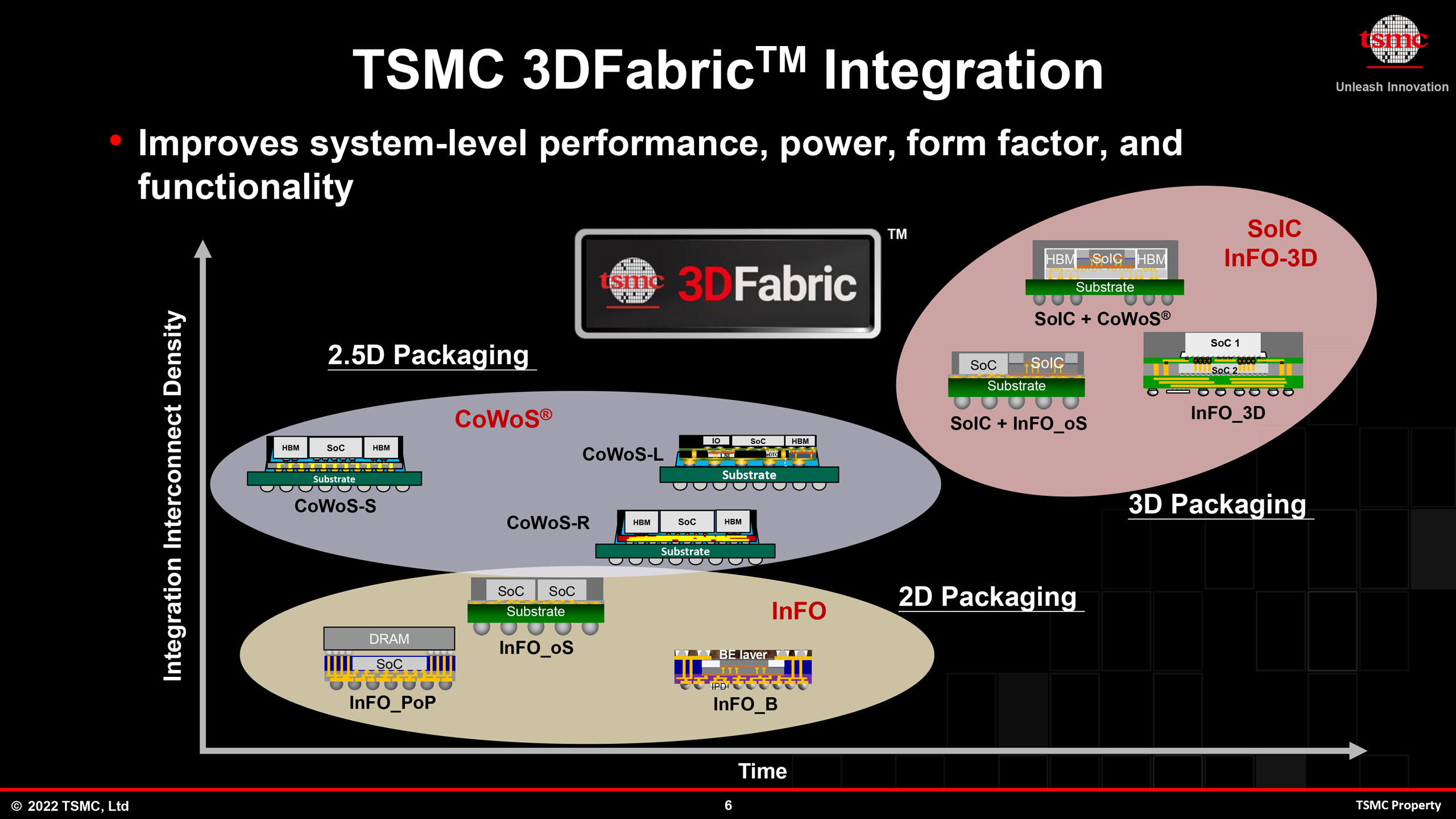
As usual, TSMC will offer their N2 node with various features and knobs to allow chip designers to optimize for things like mobile and high-performance computing designs (note that TSMC calls HPC everything that is not mobile, automotive or specialty. which includes everything from a low-power laptop CPU to a high-end compute GPU aimed at supercomputers). Also, platform offerings include something that TSMC calls 'chiplet integration', which probably means that TSMC enable its customers to easily integrate N2 chips into multi-chiplet packages made using various nodes. Since transistor density scaling is slowing down and new process technologies are getting more expensive to use, multi-chiplet packages are going to become more common in the coming years as developers will be using them to optimize their designs and costs.
TSMC expects to start risk production of chips using its N2 fabrication process sometimes in the second half of 2024, which means that the technology should be available for high volume manufacturing (HVM) of commercial products in the second half of 2025. But, considering the length of modern semiconductor production cycles, it's likely more pragmatic to expect the first N2 chips to become available either very late in 2025 or 2026, if everything goes as planned.


22 Comments
View All Comments
OreoCookie - Wednesday, June 29, 2022 - link
The issue with Intel is whether it can deliver and deliver *on time*. Intel has had persistent problems with both for years, including its next-gen chips. Until Intel starts executing like TSMC does, I don’t think it’ll be competitive.nandnandnand - Thursday, June 16, 2022 - link
Finally, some good effing food.The mixed density number is not that helpful, would rather see separate numbers. Looks like a nice efficiency gain, although it's a completely new transistor type.
lemurbutton - Thursday, June 16, 2022 - link
Why is the density increase only 1.1x compared to N3E? This seems extremely small for a full node.nandnandnand - Thursday, June 16, 2022 - link
It's an average that includes SRAM and analog scaling, so that dragged it down. Maybe they'll break it down more later.ballsystemlord - Thursday, June 16, 2022 - link
Actually, it says *greater than* 1.1. The exact scaling might not be known yet so it could grow.saratoga4 - Thursday, June 16, 2022 - link
They did the same thing when they rolled out finfets. 20nn did the shrink, then 16FF rolled out FinFETs at similar density. The idea was that changing transistor technologies is really hard so they would do it separately from the shrink. Probably similar here since GAAFETs will be a similarly complex change.name99 - Friday, June 17, 2022 - link
Because nodes are not measurements, they are “significant technology improvements”.In this case, the improvements are in transistor (GAA) and metal (backside power delivery).
The process MAY get improved lithography (and thus higher density), but that depends on ASML delivering enough high NA EUV machines on time, and TSMC don’t want to promise what they can;t be sure of, or delay GAA and backside power waiting for those machines.
Wereweeb - Friday, June 17, 2022 - link
N3 nodes are focused on getting the smallest FinFETs possible, an art that TSMC seems to have mastered, while N2 is likely focused on getting GAAFETs working with good yields to start with.It's a significantly different process, and there's no reason for them to rush it and risk crashing into a wall like Intel did with their "10nm/7". In the follow up "sub-nodes" and in the next nodes they can focus on shrinking the transistors and then rearchitecting GAAFETs to be more dense.
Doug_S - Saturday, June 18, 2022 - link
I wonder if N2 will be a node like TSMC's 10nm and 20nm where it is specifically indicated not to be a long lived node, and will have only a few customers (i.e. Apple and a few others) and most will wait for N2P or N2E or whatever they call the tweaked version.TSMC did sort of the same thing in reverse with N7, where that early version was made without EUV to remove risk but pointed most customers towards N7+ which was the less expensive version of N7 that used EUV for a few critical layers instead of SAQP.
JasonMZW20 - Tuesday, July 19, 2022 - link
I actually can't even think of any chips that used N7+ because the design rules weren't compatible with N7/N7P/N6. Maybe there were some in datacenter, but in consumer products, I'm drawing a blank.