A Visit to Intel’s D1X Fab: Next Generation EUV Process Nodes
by Dr. Ian Cutress on February 16, 2022 9:00 AM EST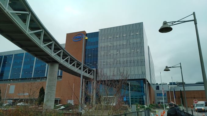
On a recent trip to the US, I decided to spend some time criss-crossing the nation for a couple of industry events and spend some of the time visiting friends and peers. One of those stops was at Intel’s D1X Fab in Hillsboro, Oregon, one of the company’s leading edge facilities used for both production and development. It’s very rare to get time in a fab as a member of the press – in the ten years covering the industry, I’m lucky to say this was my second, which is usually two more than most. As you can imagine, everything had to be pre-planned and pre-approved, but Intel managed to fit me into their schedule.
Ultimately the reason why I’d reached out in the first place to visit D1X is because Intel had sent out press invitations to visit their leading edge facility in Kiryat Gat, Israel. Intel has invited press there before, for which I couldn’t attend for family reasons, and then for the second time in a row, the timing of the Israeli fab tour wasn’t great for me – I’d be on the other side of the world at an industry conference at the time. I asked Intel if there was a way to get a fab tour elsewhere in lieu, and pieces were put into place for the Oregon trip. The irony of it all is that the Israel trip was cancelled due to Omicron COVID restrictions - although it sounds like Linus still went before the press trip for special recording. I’ll be looking forward to how his trip went.
On my visit, the site of Intel’s D1X fab is called Ronler Acres - originally a series of wetlands that Intel now preserves around the fab complex. D1X sits in Hillsboro just the other side of the airport from Intel’s Jones Farm campus. These are two of Intel’s four campuses in the region, totalling 21000 employees, or about 18% of Intel's global workforce. Understandably, the company is the biggest employer in the region, with numbers ever increasing as the facilities are built out.

Alongside me was Jeff Soleim from CraftComputing, and we arrived fresh and early at 9am – after only 4 hours sleep due to a podcast taping the night before and a 60 minute drive each way through the cold Oregonian winter morning. Jeff had kindly agreed to be a second set of eyes and ears for the trip through the fab.

Fresh Kanar, for the discerning Cardassian palette
As you might imagine, opportunities to take photos and other things inside the fab was very limited. I’d put in several requests, based on my limited knowledge of Intel’s facilities prior to visiting, however a number of elements were approved, and I’ll use those images as material through the visit. Most fabs operate a ‘no freely roaming cameras’ policy, with the mantra being that they could pick up specific customer information.
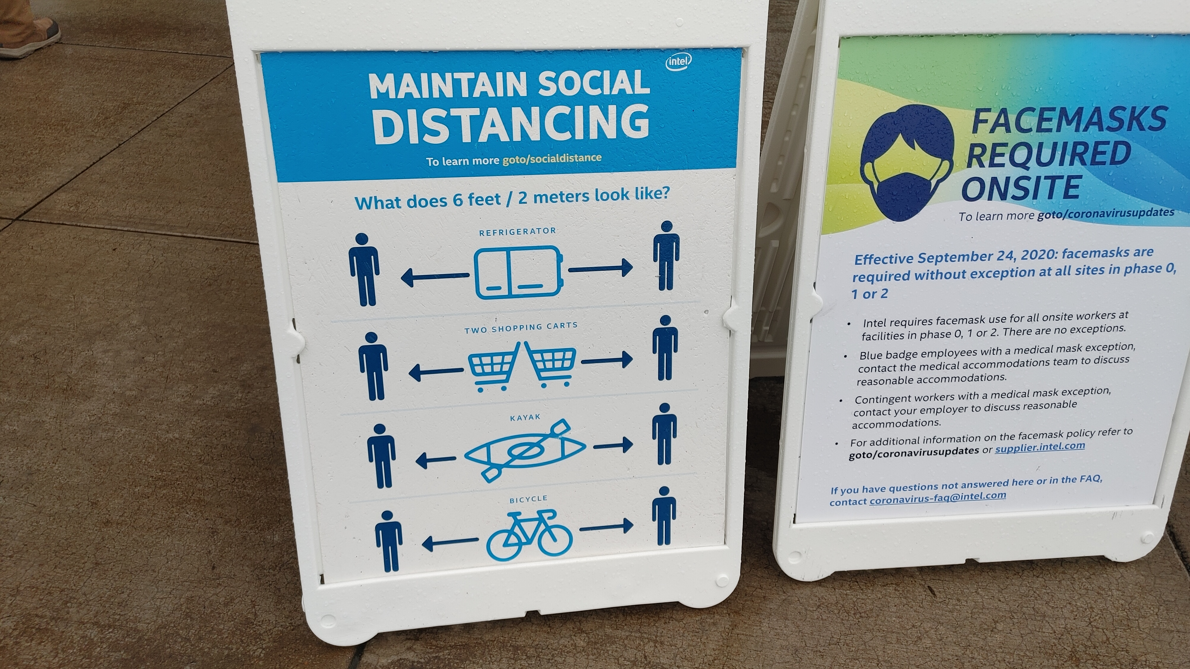
Upon approaching the Ronler Acres site, it’s worth noting that Intel’s policy at the time was to wear masks on campus at all times. There were some handy images to showcase exactly how much six feet is when it comes to social distancing.
Inside the facility is a very typical business like entrance – a front desk for employees to sign in, comfy chairs for visitors to sit in while waiting for their connections to pick them up, and walls of awards and other fancy things to showcase just how good the site is. There was also a wall about visits from former US presidents interested in semiconductors. From our perspective, it’s the walls of technology we’re interested in.

Intel is a company with lots of history when it comes to semiconductor manufacturing, and there are a number of displays like this dotted around – mostly for the visitors (like us) to bask in the technological impact that Intel has had on the industry. This diagram is pretty neat, and is going to be more exciting when it gets replaced with the one that has Intel’s first EUV, High-NA EUV, and packaging technologies. Nonetheless, we passed through the front desk, where I was given this.

I’m pretty sure I was handed the wrong badge. All Access? That’s quite dangerous.
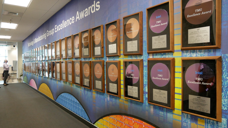
Slightly beyond the entrance is a wall of awards as part of Intel’s Manufacturing Group. From the outside, it looks like a list of accomplishments the company is giving itself, but it was interesting to see what some of them were, given that they also disclose information not previously known. Intel has requested that we don't put a list of these accomplishments as many of them are internal, but it's fun to see that there are these internal milestones relating to implementing new research, process improvements, and yield.
We were led through some office areas into a meeting room, for a small briefing ahead of our tour. As you might imagine, the tour rules are strict – don’t touch anything, stay with your chaperones at all times, and only photograph specific things we tell you that you can photograph. We had a brief overview of the site as well, Ronler Acres does manufacturing, development, packaging, and materials research all at one location. From above, the site looks like its own packaged processor with chiplets. But part of the talk was also to go through some of the PPE involved, the eponymous clean room bunny suit.
Nonetheless, before we entered the fab, we were given a safety bag.

This being full of disinfectant wipes, hand sanitizer, but also our safety glasses for the fab and specialized no-mist wipes. Everyone uses their own safety glasses for comfort in the fab, and these have to be sorted in advance due to different requirements if you have glasses. With our All Access passes, it was time to get suited up.
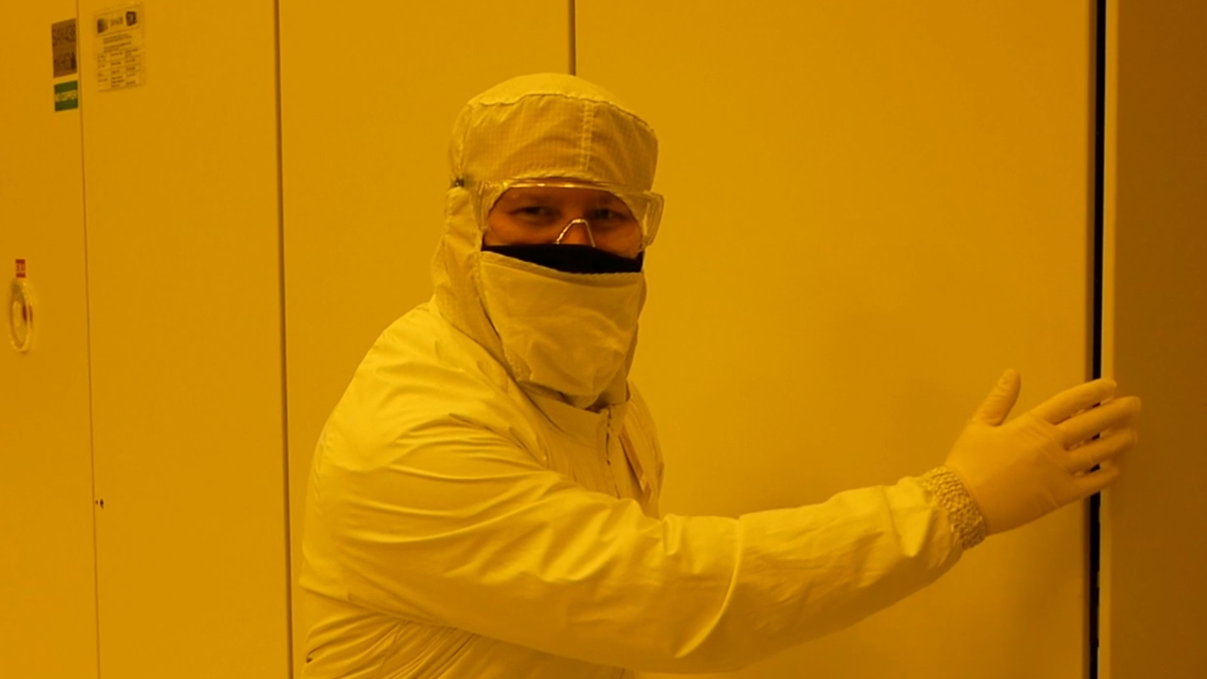
As you might imagine, wafer manufacturing is a delicate process. The clean room has to be insanely clean, and is also continuously cleaned. As a result, all the clean room equipment we have to wear is freshly laundered, and there are personal hygiene requirements too, such as limited deodorant and no hair product. I fell afoul of that last one. But the start of the process is with pre-suit gloves, beard nets, hairnets, and pre-suit boot protectors.
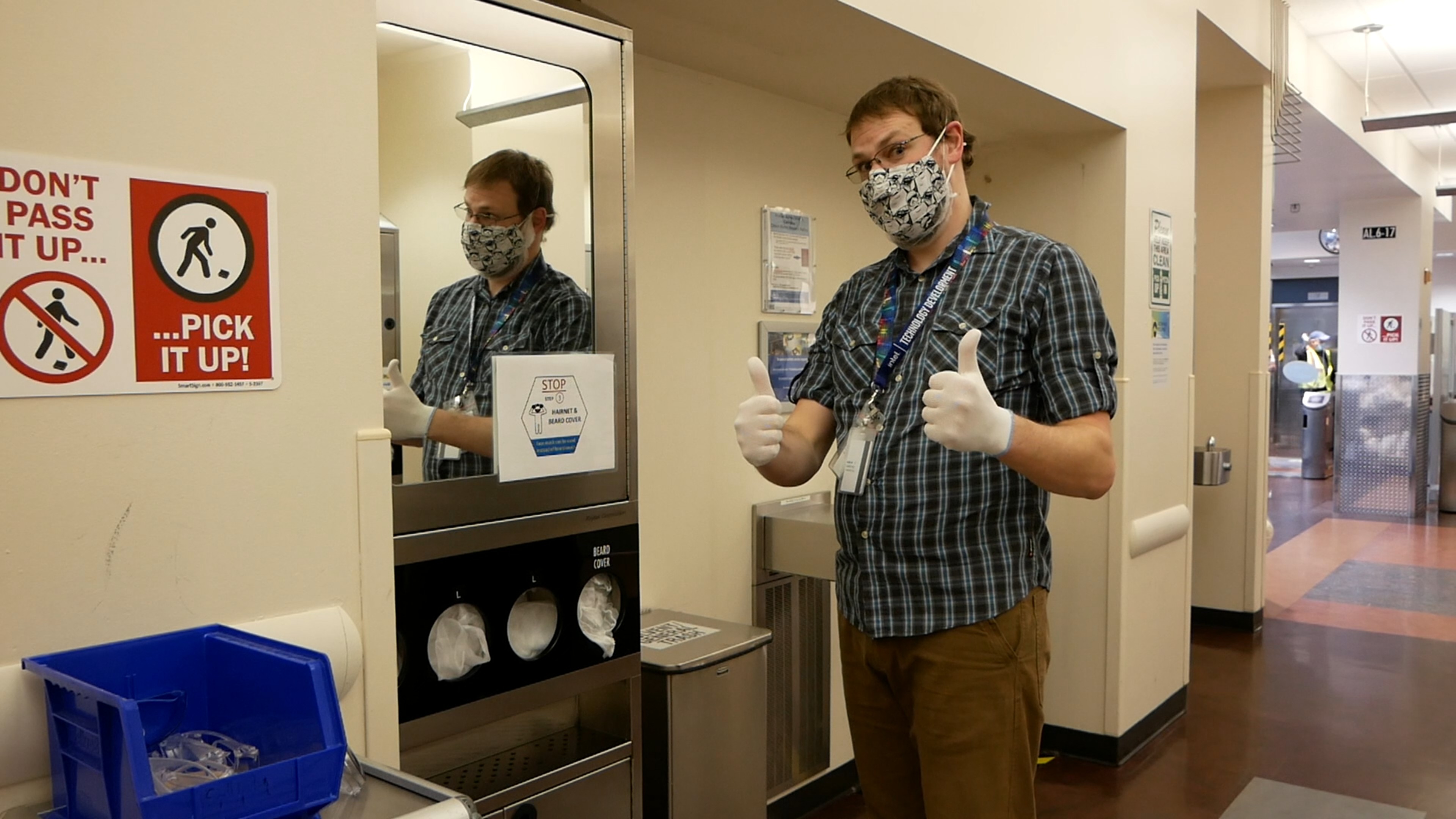
Some fabs will start with having sticky mats that you have to walk on to get rid of the dirt on your shoes, as you still wear your own shoes in the fab. This may also be coupled with forced air showers (clothes on) to help remove fluff. For us, we went straight into the rest of the bunny suit – hood, suit, more shoes. The key here is to put the suit on from the top down, with the idea being that you’re less likely to put dust and particulates on yourself this way. The full ‘bunny suit’ getup, minus the last vinyl gloves, looks something like this:
![]()
Each of the different parts comes in multiple sizes, and is always a bit of guesswork converting from what I think is a medium to what the fab thinks is a medium. The final part of the suit is a double check up and down in the mirror, also with a colleague if you have one, to make sure going into the fab that everyone is suited and booted. Then, we go in.
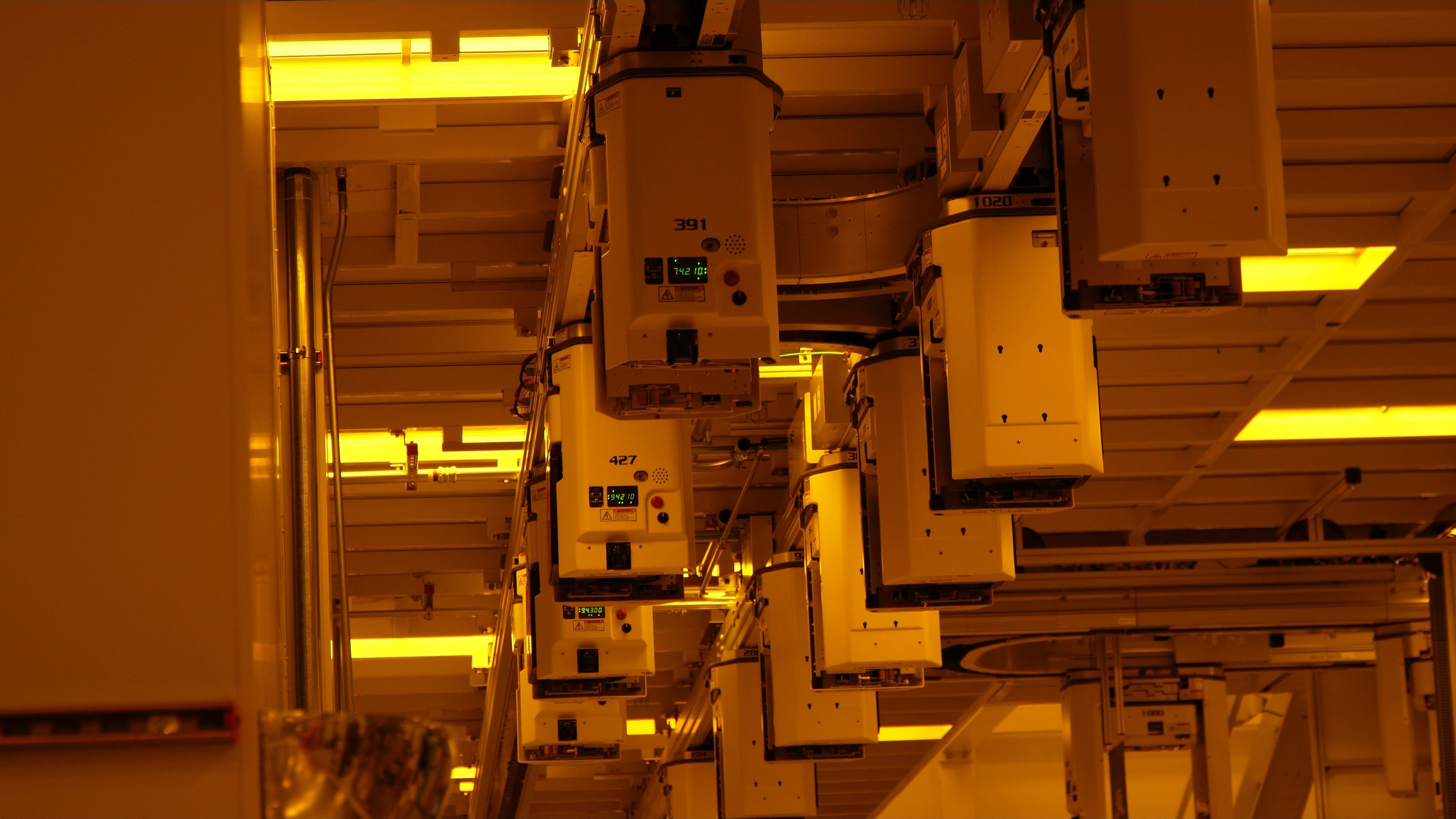
If you’ve never been in a fab before, then the first thing you notice is that everything on the clean room floor is yellow. This is by design – the yellow sodium lights reduce the number of wavelengths of light in the room, to stop any of them potentially interacting with the wafers that are in transit.
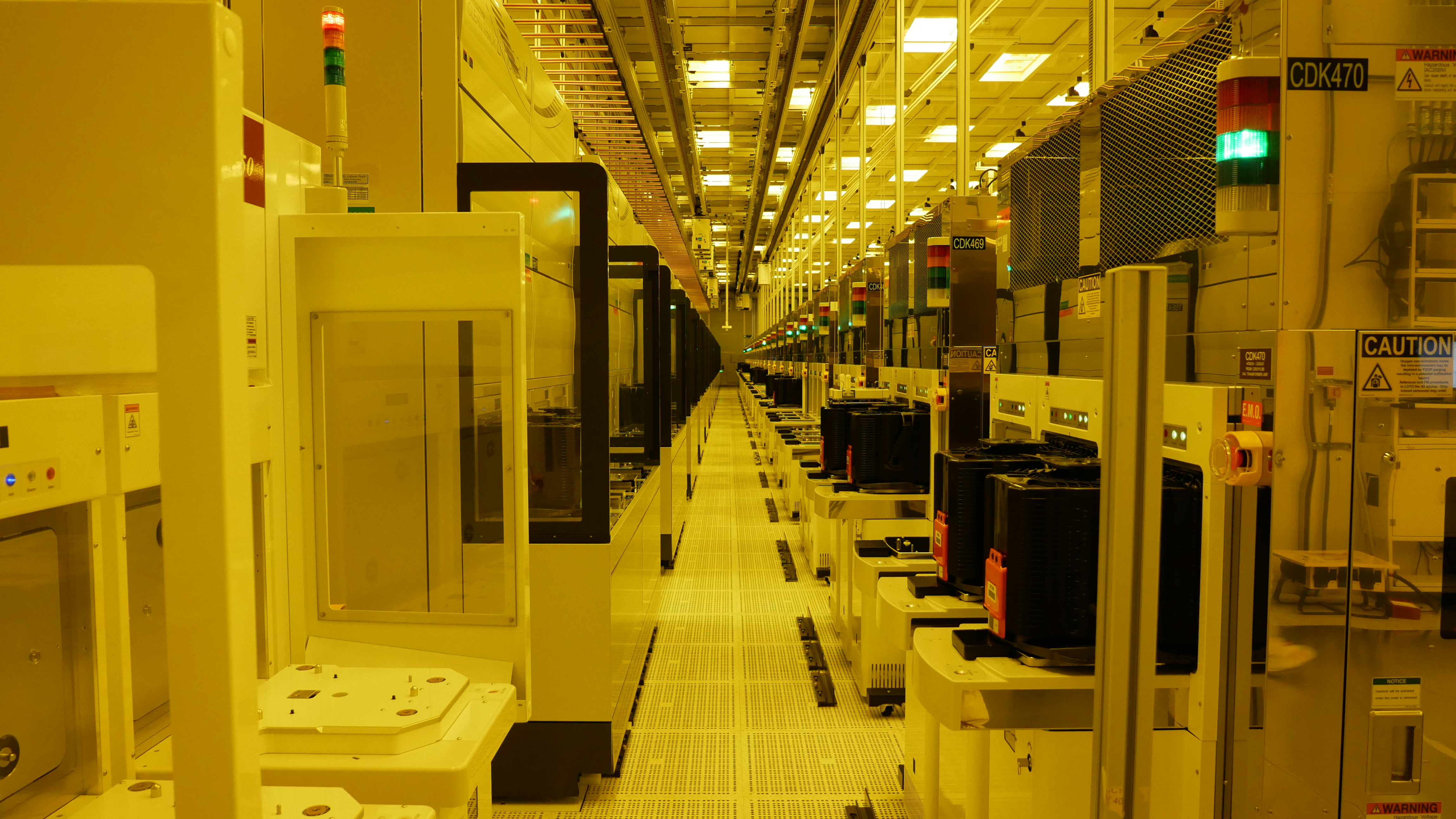
The size of the fab is enormous, we’re talking football pitches upon football pitches (doesn’t matter if you mean American or Rest of World football). A fab like this, in order to be profitable, has to scale. That means not only 20 similar machines deep, but hundreds of different machines wide, depending on the processes needed. If each processor requires 80-120 masking steps to be made, then each of those masking steps requires deposition, lithography, etching, cleaning, and inspecting. The machines for each of these steps cost from a million to hundreds of millions for the big EUV machines.

A line of EUV machines
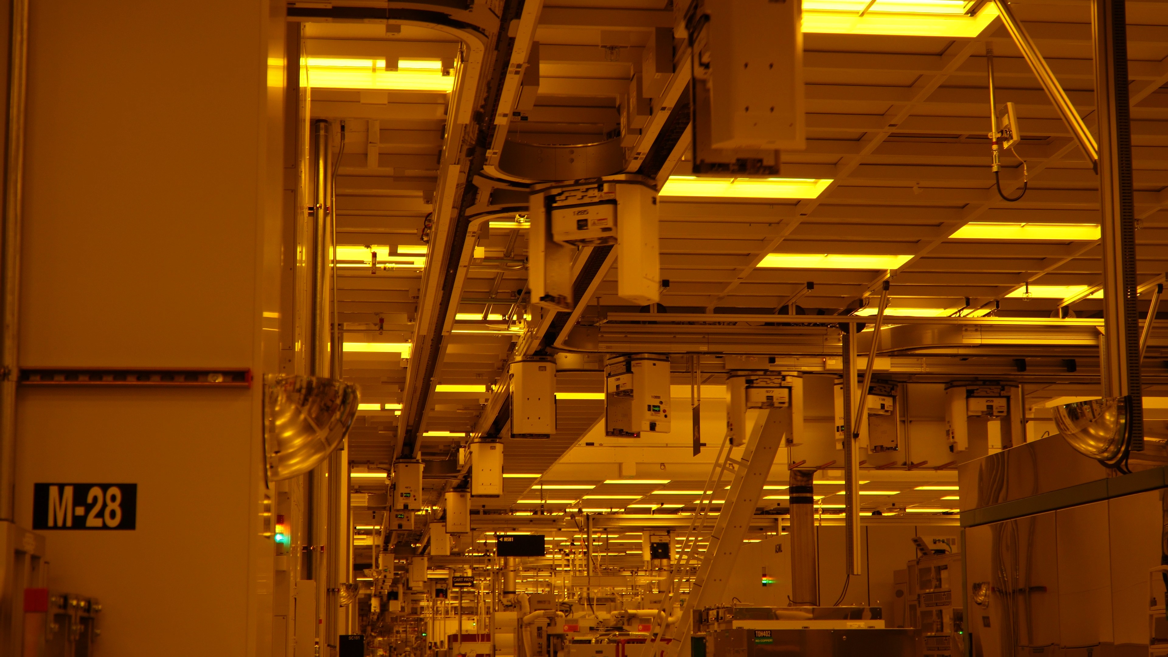
One thing you will notice when you go into a fab is also how tall it is. These buildings are designed to be autonomous but also easy to maximize uptime. That means if something fails (like a ceiling light), it can be repaired without disabling anything. Even the ceiling lights have access from above the fab if they ever need to be repaired or replaced. But the reason why the fab area is so tall is because some of the machines are two stories high, especially the EUV machines. Sometimes these have to be lifted in, or use reinforcement beams to install them. It’s quite hard to miss.
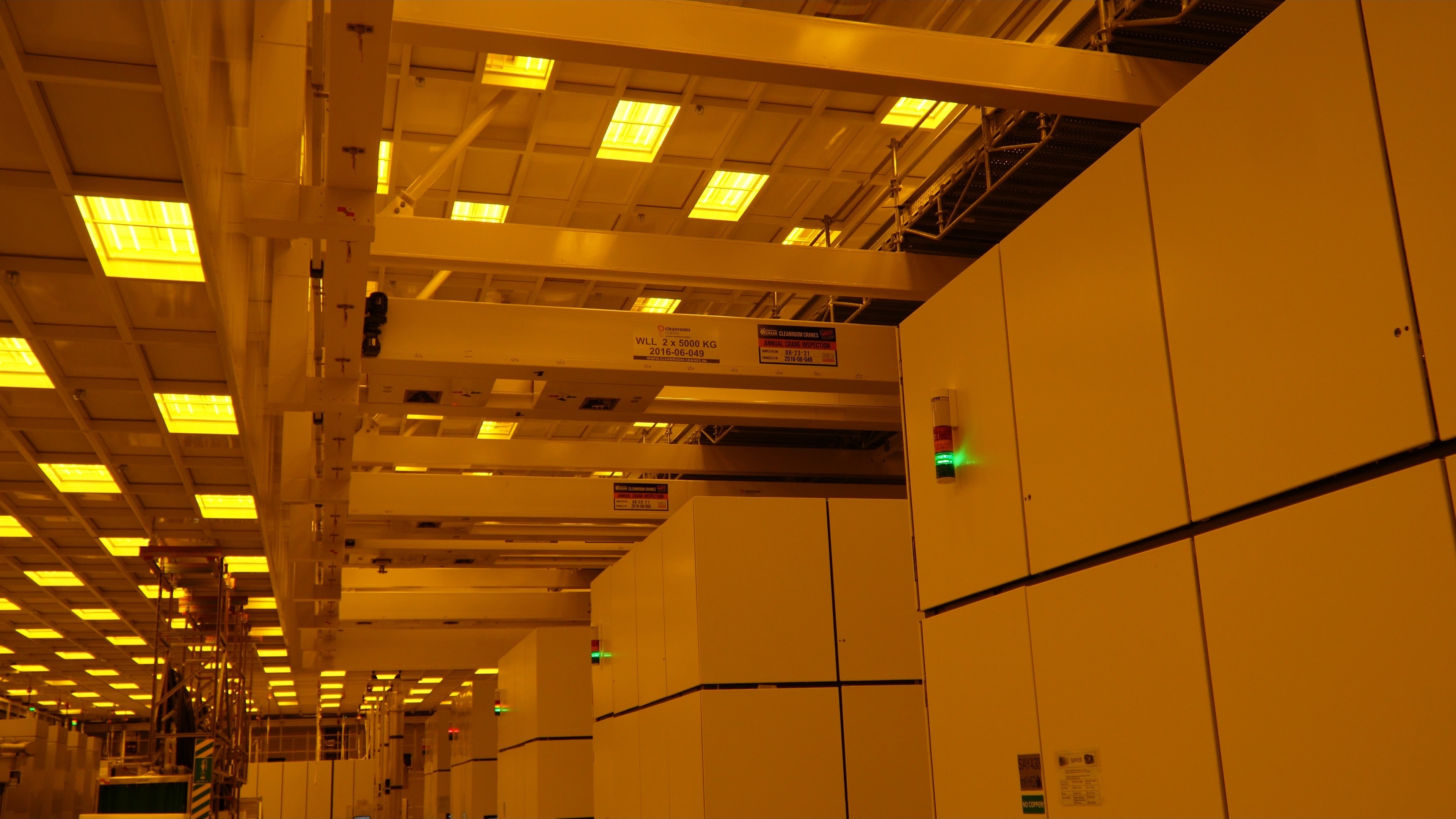
Each machine also needs chemicals and electricity, which is provided underneath in the sub-fab. While I’ve been in a sub-fab before, we weren’t able to on this visit, but the sub-fab is as big as the clean room itself, if not bigger. I was told that an EUV machine requires 6x more sub-fab space than clean room space, showcasing that sometimes when it comes to raw square footage, what you need to support these machines requires more than the machine itself.
The fab has a very slight positive air pressure which is noticeable. The fab pushes air from the ceiling to the floor, through the vents you see on the images above. This is also to reduce dust and particulates, and drive them down and away to be cleaned rather than up into the air where they might fall down.
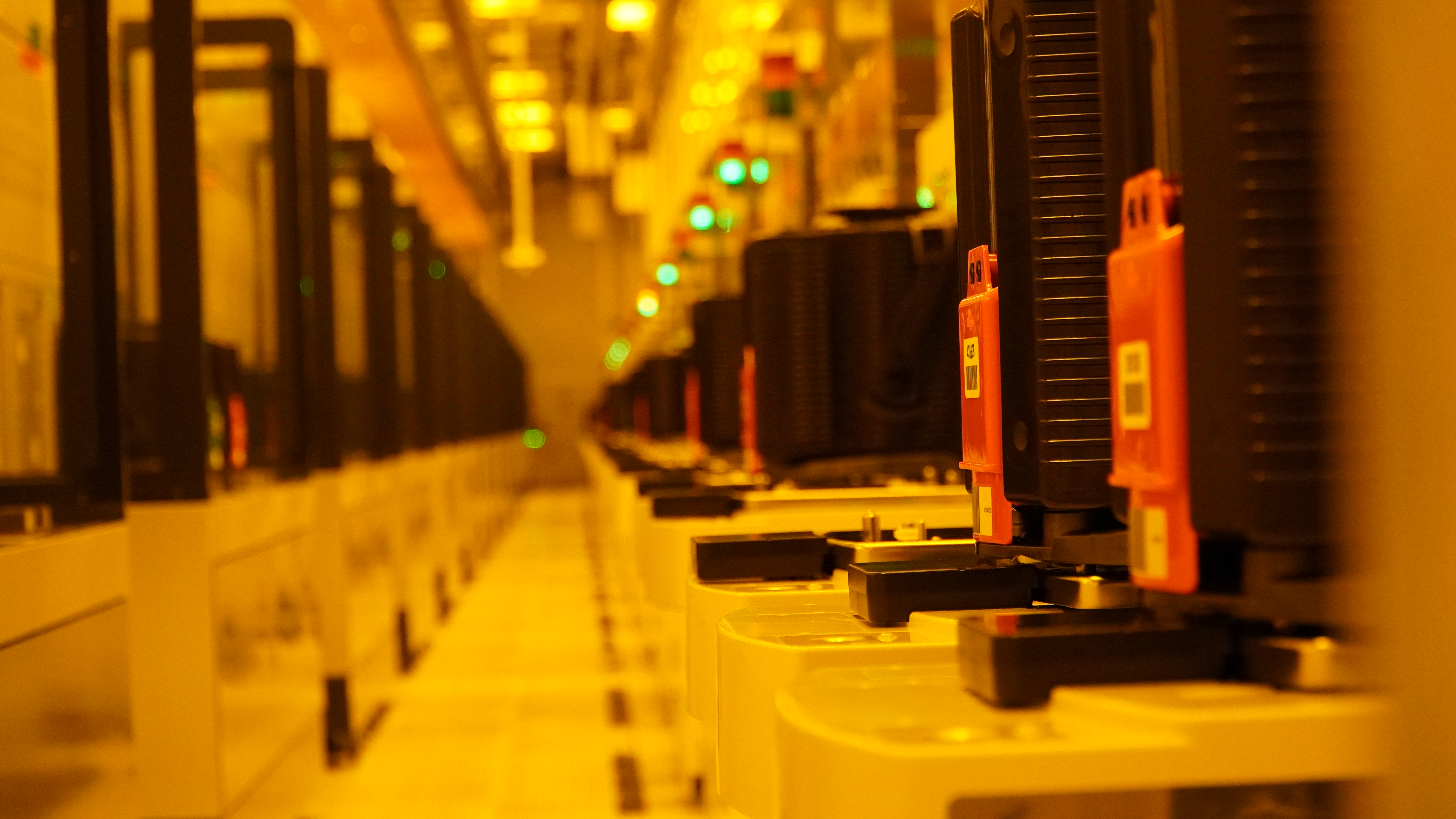
It’s important to note that the wafers aren’t meant to be exposed to the air at all. Wafers travel in batches of 25 inside a FOUP (front opening unified pod), which are carried around the fab on the pod highway sitting above the machines. This is all tracked and automated, so when a FOUP is complete at one machine, it is picked up by an automated pod and either taken to the next machine, or put back into storage waiting for the next stage in the chip creation.
It’s hard to say how many of these automated pod carriers there were – we saw three figure numbers on each one, which means there might be up to 1000 in this facility alone. The pod ‘highway’ stretches the length of the Ronler Acres site, from storage to fab to packaging. They are designed to be self-reporting if there’s an error, or if one brakes down, the system can re-route around it until it is physically addressed. Most of the FOUPs are black to minimize light, however some machines have see-through windows that you can look into.
Jeff and I were able to look into a couple of machines like this, with the machine taking wafers out of the FOUP for photoresist application (we think). The wafers we saw already had a lot of the regular markings on them for a processor – it looked like an 8-core design, with zero E-cores, so who knows what we were looking at. On another machine, one of the metrology (inspection) machines, we saw a wafer representation on one of the monitors with a diagram of each of the dies on the wafer. For those of you who read AnandTech often, you’ll know that I like die area calculations with simple wafer images – from the back-of-the-brain mathematics I was able to deduce we were looking at a leading edge wafer with ~400mm2 die area. I'll leave you to imagine what that might be.
One thing worth noting is that there were lots of people in the fab. The last one I visited, Fab 8 of GlobalFoundries in upstate NY, there were barely two dozen people in the same space. Here at Intel, I could see dozens, if not over a hundred. This is because D1X is a development fab, so not only is the silicon in development and being monitored, but also D1X is expanding its capacity with the Mod 3 expansion. This means that people were installing hardware in the final third of the building, including EUV machines.
So it’s no secret that Intel is yet to productize its EUV technology. Despite being one of the early developers, it wasn’t ready for 10nm and it didn’t fit into the process easily, so we’re going to see it on Intel 4 at a later date. But that doesn’t mean that Intel has sat on its laurels – inside the fab we saw a number (which I’m not able to disclose) of EUV machines in various states of undress. In one of the beginning sections of the fabs, the EUV machines were fully clothed.
 Touching an EUV machine. I had to ask. Nicely.
But in others, they were still being installed. As you might imagine, I wasn’t allowed to take pictures of an EUV machine being installed, but looking inside the thing was somewhat mind-blowing. I’m not sure exactly what part I was looking at, but there were plenty of pipes with labels such as ‘Noble Gas’, all part of what looked like a 2 meter wide machined aluminium half-sphere. Everything inside felt bespoke for the machine, and when you realize one of these things has over 100,000 different components and takes six months to install, plus another six months to tune, you can see why. I think I spent a good few minutes just looking in awe, before wanting to actually understand what was going on. I think it was on the fifth shout from our chaperone to keep moving that I finally came back into the real world. I feel somewhat sad that I can’t share with you what I saw, as words do not do it justice.
Aside from the yellow-light section of the fab, Intel also had a part of the fab under regular lighting – we didn’t spend much time in there, and Intel didn’t go into too much detail what that part of the fab was, but it was a lot more cramped in that space. Machines were so close together there wasn’t a clear path for us to walk down. On the way back however, I did notice a machine that had lots of warning hazard labels of a variety of harsh chemicals – hydrogen fluoride, various sulfurous components combined with halogens, and even some aggressive silicate compounds, designed for use in etching and cleaning. Teaching sand to think requires lots of aggressive chemicals, which Intel says it puts a lot of effort into reusing what it can and recycling everything else.
More FOUP Action. It was quite loud in the fab
Overall, we spent about 90 minutes in the fab, including a spot or two for pictures and a minute or ten for die-size calculations based on what we could see on monitors that we couldn’t photograph. The good thing about visiting a fab is that you’re visiting a fab – the bad thing is that without visiting it first and knowing what you’ll get to see, it’s hard to prepare in advance or research in advance what’s there, what questions to ask, and if there’s any content for an audience looking through the keyhole for the slightest glimpse. I’m the sort of person who will happily stand and investigate each machine for 90 minutes to understand how it works – its one thing to read the research papers at industry conferences on how the manufacturing works, but another to actually see it up close.
There’s also another perspective here. I know that if I had been in a not-so-cutting-edge facility, something 45nm, 90nm or even older, I’d have the same response. I wouldn’t be looking inside EUV machines, but I would still want to know how everything worked, seeing wafers flying over the place, and knowing that these machines are doing the most physics-bending things possible to get something simple like a car-seat controller onto the market.
I’ve asked Intel if I can go visit whichever fab is getting the High-NA machine installed when it’s ready - I’m told that it’s bigger than regular EUV, so I can’t wait to see it. Being so far out, I wasn’t expecting a steadfast commitment, but no doubt I’ll reach out as it gets closer to time. Many thanks to Intel for letting me run riot in one of the most expensive rooms on the planet.
On a side note, I’ve now visited GlobalFoundries and Intel. There were plans for a press trip to go visit Samsung, but those were washed away by the pandemic in early 2020 – I’m hoping the opportunity comes around again when we’re all in a safer environment. The odd one out then is TSMC, which according to a number of sources, has never had a tech press tour of its facilities – TSMC let the BBC come for a short filming session at Fab 12 (leading edge) in late 2019, although the short video was little more than a ‘wow chips’ moment for that audience. If anyone from TSMC is reading this, and we get traveling again, I’d love to get the opportunity to connect in person to do something for the technical community.


38 Comments
View All Comments
dwillmore - Wednesday, February 16, 2022 - link
Grammar error: " or if one brakes down," Breaks is the correct word. I guess one could break down by braking down, but that's probably not what you meant.Mike Bruzzone - Wednesday, February 16, 2022 - link
mbprophet001 - Wednesday, February 16, 2022 - link
Super cool write-up. Thanks!thestryker - Wednesday, February 16, 2022 - link
Love the fab trips even if they aren't able to give you any specifics as it's super interesting stuff that we rarely get a glimpse into.EUV + 8p0e would hint at perhaps Meteor Lake since I believe those are not only the first on an EUV node, but also using the tile packaging.
MananDedhia - Wednesday, February 16, 2022 - link
Brings back memories of when I worked in GF Fab 8. Thank you for the article.Drkrieger01 - Wednesday, February 16, 2022 - link
This is why I read this website:"If anyone from TSMC is reading this, and we get traveling again, I’d love to get the opportunity to connect in person to do something for the technical community."
It's these ideas to connect with big silicon companies, showing us what all is inside and exciting new generations to leap into the silicon field. I wish I had seen stuff like this when I was going through school, it would have cemented my path into computer engineering :)
fmcjw - Thursday, February 17, 2022 - link
CDC is talking about opening up borders for business travel in 2H22 to Taiwan, and a site visit will be one of the best "applications" of that policy. Wish you success.DanNeely - Thursday, February 17, 2022 - link
Ian's in the UK, so it'd need to be their govt moving not the USA's. Oh and Taiwan's of course. From the twitter sidebar yesterday they still have a really long quarantine on arrival period that's prohibitive for most travelers.CajunArson - Wednesday, February 16, 2022 - link
"For those of you who read AnandTech often, you’ll know that I like die area calculations with simple wafer images – from the back-of-the-brain mathematics I was able to deduce we were looking at a leading edge wafer with ~400mm2 die area. I'll leave you to imagine what that might be."Sapphire Rapids tiles.
watersb - Wednesday, February 16, 2022 - link
Wow!