Intel's Process Roadmap to 2025: with 4nm, 3nm, 20A and 18A?!
by Dr. Ian Cutress on July 26, 2021 5:00 PM ESTSidebar on Intel EUV
In all of these announcements, one thing to highlight is Intel mentioning its relationship with ASML, the sole company that manufactures the EUV machines powering production of leading edge semiconductor manufacturing.
ASML Wilton
ASML is a unique company in that it is the only one that can produce these machines, because the technology behind them is often tied up with its partners and research, but also because all the major silicon manufacturers are heavily invested in ASML. For any other company to compete against ASML would require building a separate network of expertise, a decade of innovation and design, and a lot of capital. None of the major silicon vendors want to disturb this balance and go off on their own, lest it shuts them out of the latest manufacturing technology, and no research fund sees competing against the embedded norm as a viable opportunity. This means that anyone wanting EUV specialist technology has to go to ASML.
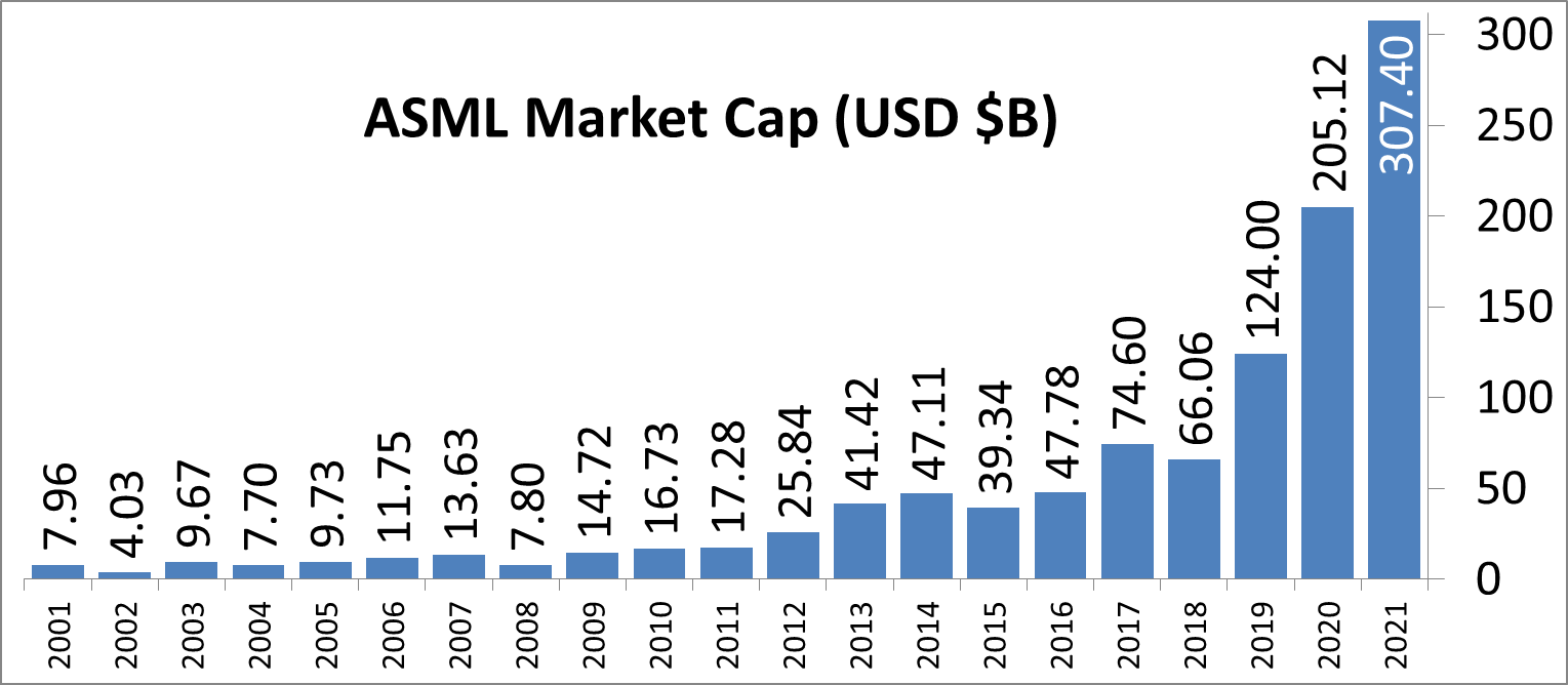
In 2012, it was reported that Intel, Samsung, and TSMC all invested in ASML. This was, at the time, to jumpstart EUV development along with migrating from 300mm wafers to 450mm wafers. While we haven’t moved to 450mm wafers yet (and there are doubts we will any time in the next decade), EUV is now here. Intel’s 2012 investment of $2.1 billion gave them a 10% stake in ASML, with Intel stating that it would continue investing up to a 25% stack. Those stakes are now below the 5% reporting threshold, but all three of the major foundry customers are still big owners, especially as ASML’s market cap has risen from $24 Billion in 2012 to $268 Billion in 2021 (surpassing Intel).
As major investors but also ASML’s customers, the race has been on for these foundries to acquire enough EUV machines to meet demand. TSMC reported in August 2020 that it has 50% of all EUV machines manufactured at ASML for its leading edge processes. Intel is a little behind, especially as none of Intel’s products in the market yet use any EUV. EUV will only intercept Intel’s portfolio with its new Intel 4 process, where it will be used extensively, mostly on the BEOL. But Intel still has to order machines when they need them, especially as there are reports that ASML currently has backorders of 50 EUV machines. In 2021, ASML is expected to manufacture around 45-50 machines, and 50-60 in 2022. The exact number of machines Intel has right now, or has ordered from ASML, is unknown. It is expected that each one has a ~$150m price tag, and can take 4-6 months to install.

With all that being said, Intel’s discussion point today is that it will be the lead customer for ASML’s next generation EUV technology known as High-NA EUV. NA in this context relates to the ‘numerical aperture’ of the EUV machine, or to put simply, how wide you can make the EUV beam inside the machine before it hits the wafer. The wider the beam before you hit the wafer, the more intense it can be when it hits the wafer, which increases how accurately the lines are printed. Normally in lithography to get better printed lines, we move from single patterning to double patterning (or quad patterning) to get that effect, which decreases yield. The move to High-NA would mean that the ecosystem can stay on single patterning for longer, which some have quoted as allowing the industry to ‘stay aligned with Moore’s Law longer’.
| ASML's EUV Shipments | |||||||||||||||||||||
| 2015 | 2016 | 2017 | 2018 | 2019 | 2020 | 2021 | |||||||||||||||
| Actual | 2 | 4 | 10 | 3 | 4 | 5 | 6 | 4 | 7 | 7 | 8 | 4 | 7 | 14 | 8 | 7 | 9 | - | - | ||
| Target (Total) | - | - | - | 20 (18) | 30 (26) | 35 (33) | 45-50 | ||||||||||||||
| 2018 and beyond is split per quarter for actual shipped numbers Data taken from ASML's Financial Reports |
|||||||||||||||||||||
Current EUV systems are NA 0.33, while the new systems are NA 0.55. ASML’s latest update suggests that it expects customers to be using High-NA for production in 2025/2026, which means that Intel is likely going to be getting the first machine (ASML NXE:5000 we think) in mid-2024. Exactly how many High-NA machines ASML intends to produce in that time frame is unknown, as if they flood the market, having the first won’t be a big win. However if there is a slow High-NA ramp, it will be up to Intel to capitalize on its advantage.


326 Comments
View All Comments
bigboxes - Tuesday, July 27, 2021 - link
Yeah, Intel is still king of the liars. I've got a box full of Intel CPUs, but Intel really crapped the bed. Intel 7 is the new 10nm. Can't make this stuff up! We can't put out a competitive product so we'll call it 7 anyways! GO INTEL GO!Geef - Saturday, July 31, 2021 - link
At least Intel is consistent. They have consistently added a + to their 14nm chips every single year!mode_13h - Sunday, August 1, 2021 - link
:Daovander - Tuesday, August 3, 2021 - link
Which is exactly what TSMC did with their 14nm node.This was how the whole naming problem got started but no one seemed to care since it seemed like they were catching up to Intel and all the Intel haters were happy to see it.
When Intel shocked the world and released its FinFET (Tri-Gate) process at 22nm TSMC followed it with the horrible 20nm planar node though it had lower transistor density than Intel 22nm. TSMC was claiming its 20nm node was a half shrink of the 22nm node and therefore meant they were keeping up with Intel. TSMC felt they were justified in this because Intel 22nm transistor density missed the target of a full node shrink by a bit with the introduction FinFET's. This was a consequence of the new trench contact structure required between the Fin’s and Metal 0. TSMC has the same problem when they introduce Fin’s. Then, Intel released 2nd Gen FinFET, the 14nm node, with more than a full node of shrinkage to get back on track with what they missed at 22nm.
TSMC then released their 14nm node shortly after with the same backend as the 20nm node - so no transistor density scaling, it was the same node really (sound familiar). Then, Intel got over-optimistic and tried to scale more than a full node again using Spacer Quad patterning at 10nm and got stuck in a 6 year delay. At the same time they decided to pass on using EUV for 10nm because at the time it was not ready for production.
TSMC bought up all the EUV steppers in the world and then proceeded down the lithographic scaling trail of 10nm, 7nm, 5nm, and soon 3nm. A smart move on their part and easier to make since the throughput of the EUV tool increased in the meantime (since they were a bit behind Intel in that development decision). Essentially all this scaling was handed to them on a silver platter by ASML. Also, the transistor density of these 3-4 nodes has been well off the traditional density shrink which is why Intel 2 nodes (or more depending on how you interpret the marketing names) still has a density that matches them.
They did not produce any real innovations in any of those nodes. Gate-all-around has been the obvious next step for 5-6 years. If they were "innovating" all this time with all these new nodes why did they not develop this. Now we see everyone claiming to have it ready to go in the 2024-2025 timeframe since IBM made their 2nm announcement. Funny how that is, wonder where everyone is getting it from?
All I am saying is, if you are going to call Intel a Liar then you have to call everyone else one first.
Given the confusion in the industry and the desire to truly compare technologies names with matched Transistor density, the whole world pushed Intel into changing their naming scheme since there was no possibility of getting the foundries to go backwards.
mode_13h - Wednesday, August 4, 2021 - link
@aovander thanks for the info.As I've said several times, Intel can just name their node with a monotonically increasing sequence that has no obvious or direct relation to density. Just opt out of the whole nm race, entirely.
Dex4Sure - Tuesday, November 23, 2021 - link
Intel's 10nm is actually slightly better than TSMC's 7nm in density... So they may as well call it "Intel 7".Butterfish - Tuesday, July 27, 2021 - link
Any proof? Or just pulling thin air out of your arse to satisfy your agenda? The density comparison graph in the first page of this article literally disapprove your statement.Spunjji - Wednesday, July 28, 2021 - link
@Butterfish - not to agree with DigitalFreak here, but it's worth noting that Intel haven't actually managed to produce a shipping design anywhere near their quoted density for 10nm, while TSMC customers (most notably AMD) have come much closer to their quoted density.I'd still say that 10ESF looks broadly comparable to TSMC 7nm, though - much moreso than Samsung's 8nm.
Butterfish - Thursday, July 29, 2021 - link
Yes they have. The Cannon Lake Core i3-8121U did use the high density libraries that has the advertised maximum density for 10nm.Spunjji - Friday, July 30, 2021 - link
@Butterfish - You're citing the broken chip that only shipped in one cut-price notebook; one that doesn't have public figures for transistor count available, so we don't know anything for sure about the density. The possibilities are either that you're technically correct in the worst way - i.e. they haven't shipped anything that /worked properly/ with their quoted 100M density - or you're wrong on both counts. 🤷♂️Back in the world of numbers we know for sure, Lakefield hit almost exactly 49% of their quoted 10nm density, and that had all the inconvenient I/O stuff shunted off to its secondary die.