Using AI to Build Better Processors: Google Was Just the Start, Says Synopsys
by Dr. Ian Cutress on June 23, 2021 9:00 AM EST
In an exclusive to AnandTech, we spoke with Synopsys’ CEO Aart de Geus ahead of a pair of keynote presentations at two upcoming technical semiconductor industry events this year. Synopsys reached out to give us an overview of the key topic of the day, of the year: as part of these talks, Aart will discuss what was considered impossible only a few years ago – the path to finding a better and automated way into chip design through the use of machine learning solutions. Within the context of EDA tools, as Google has demonstrated recently, engineers can be assisted in building better processors using machine learning algorithms.
The Modern Push-Pull Economics of Better Data Analysis Tools
If you read mainstream columns about technology and growth today, there is an eminent focus on the concepts of big data, artificial intelligence, and the value of analyzing that data. With enough data that has been analyzed effectively, companies have shown that they are proactive to customers, predict their needs in advance, or identify trends and react before a human has even seen the data. The more data you have analyzed, the better your actions or reactions can be. This has meant that analyzing the amount of data itself has intrinsic value, as well as the speed at which it is processed. This has caused an explosion of the demand for better analysis tools but also an explosion in data creation itself. Many senior figures in technology and business see the intersection and development of machine learning data analysis tools to churn through that data as the mark of the next generation of economics.
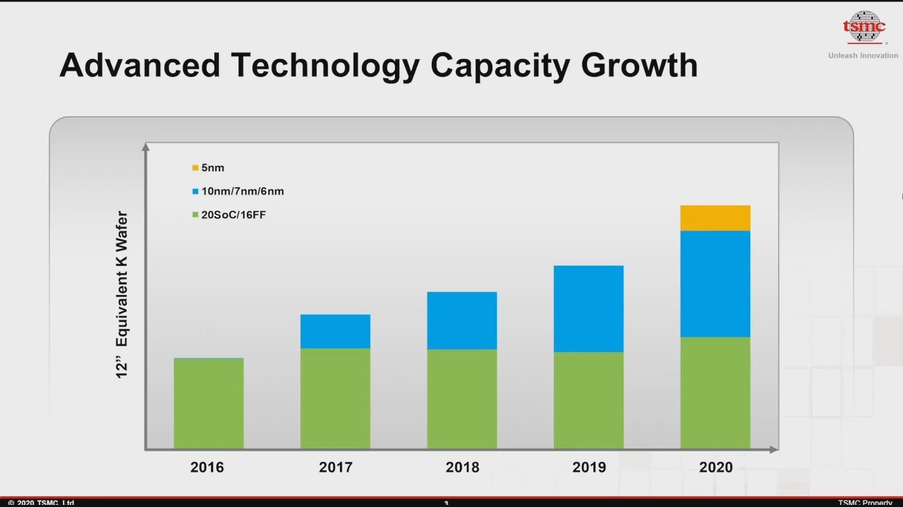
Graph showing manufacturing growth of key silicon product lines since 2016
at TSMC, the world's largest contract manufacturer
The desire to have the best solution is accelerating the development of better utilities, but at the same time, the need to deploy it at scale is creating immense demand for resources. All the while, a number of critics are forecasting that Moore’s Law, a 1960s observation around the exponential development of complex computing that has held true for 50 years, is reaching its end. Others are busy helping it to stay on track. As driving performance requires innovation on multiple levels, including hardware and software, the need to optimize every abstraction layer to continue that exponential growth has become more complex, more expensive, and requires a fundamental economic gain to those involved to continue investment.
One of the ways in driving performance on the hardware side is in designing processors to work faster and more efficiently. Two processors with the same fundamental building blocks can have those blocks placed in many different orientations, with some arrangements beneficial for power, others for performance, or perhaps for design area, while some configurations make no sense whatsoever. Finding the best combination in light of the economics at the time is often crucial to the competitiveness of the product and the buoyancy of the company that relies on the success of that product. The semiconductor industry is rare in that most chip design companies effectively bet the entire company on the success of the next generation, which makes every generation's design more important than the last.
Humans are Slow, Brute Force is Impossible, But AI Can Help
In light of the rate of innovation, chip design teams have spent tens of thousands of hours honing their skills over decades. But we are at a stage where a modern complex processor has billions of transistors and millions of building blocks to put together in something the size of a toenail. These teams use their expertise, intuition, and nous to place these units in the best configuration, and it gets simulated over the course of 72 hours. The results that come through are analyzed, the design goes back to be updated, and the process repeats. Getting the best human-designed processor in this fashion can take six months or more, because the number of arrangements possible is equivalent to the number of atoms in the known universe… risen to the power of the number of atoms in the known universe. With numbers so large, using computers to brute force the best configuration is impossible. At least, it was thought to be.
Work from Google was recently published in the scientific journal Nature about how the company is already using custom AI tools to develop better silicon, which in turn helps develop better custom AI tools. In the research paper, the company applied machine learning algorithms to find the best combination of power, performance, and die area for a number of test designs.
In order to reduce the complexity of the problem, Google limited its scope to certain layers within the design. Take, for example, an electrical circuit that is designed to add numbers together - in Google’s work, rather than try and find the best way to build a circuit like this every time, they took a good adder design as a fundamental building block of the problem, mapped how it interacts with other different fundamental blocks, and then the AI software found the best way to build these fundamental blocks. This cuts down the number of different configurations needed, but the problem is still a difficult one to crack, as these blocks will interact with other blocks to varying degrees based on proximity, connections, and electrical/thermal interactions. The nature of the work always depends on what level of abstraction these different building blocks take, and how complex/basic you make them.

Simple 8-stage example of block placement and routing affects the design choices
In Google’s paper, the company states that their tools have already been put to use in helping design four parts of an upcoming Google TPU processor designed for machine learning acceleration. While the paper showcases that AI tools weren’t used across the whole processor, it is taking some of the work that used to be painstaking in engineer labor hours and accelerating the process through computation. The beauty of this application is that the way these building blocks can be put together can scale, and companies like Google can use their datacenters to test thousands of configurations in a single day, rather than having a group of engineers provide a handful of options after several months.
Google’s approach also details the effect of using optimized machine learning (so algorithms that have learned how to be better by examining previous designs) against fresh machine learning (algorithms with only a basic understanding that learn from their own trial and error). Both these areas are important, showcasing that in some circumstances, the algorithms do not need to be pre-trained but can still deliver a better-than-human result. That result still requires additional validation for effectiveness, and the results are fed back into the software team to create better algorithms.
There's More To Come, and It Starts with EDA
But this is just the tip of the iceberg, according to Synopsys CEO Aart de Geus, whose company's software helps develop more silicon processing intellectual property in the industry today than anyone else. Synopsys has been involved in silicon design for over 35+ years, with hundreds of customers, and its latest AI-accelerated product is already in use at a number of high-profile silicon design teams making processors today to help accelerate time to market with a better semiconductor placement than humans can achieve.
Synopsys is a company that makes ‘EDA’ tools, or Electronic Design Automation, and every semiconductor company in the industry, both old and new, relies on some form of EDA to actually bring silicon to market. EDA tools allow semiconductor designers to effectively write code that describes what they are trying to make, and that can be simulated to sufficient accuracy to tell the designer if it fits within strict parameters, meets the requirements for the final manufacturing, or if it has thermal problems, or perhaps signal integrity does not meet required specifications for a given standard.
EDA tools also rely on abstraction, decades of algorithm development, and as the industry is moving to multi-chip designs and complex packaging technologies, the software teams behind these tools have to be quick to adapt to an ever-changing landscape. Having relied on complex non-linear algorithm solutions to assist designers to date, the computational requirements of EDA tools are quite substantial, and often not scalable. Thus, ultimately any significant improvement to EDA tool design is a welcome beacon in this market.
For context, the EDA tools market has two main competitors, with a combined market cap of $80B and a combined annual revenue of $6.5B. All the major foundries work with these two EDA vendors, and it is actively encouraged to stay within these toolchains, rather than to spin your own, to maintain compatibility.
Synopsys CEO Aart de Geus is set to take the keynote presentations at two upcoming technical semiconductor industry events this year: ISSCC and Hot Chips. As part of these talks, Aart will discuss what was considered impossible only a few years ago – the path to finding a better and automated way into chip design through the use of machine learning solutions. Within the context of EDA tools, as Google has demonstrated publicly, engineers can be assisted in building better processors, or similarly not so many engineers are needed to build a good processor. To this point, Aart’s talk at Hot Chips will be titled:
‘Does Artificial Intelligence Require Artificial Architects?’
I spent about an hour speaking with Aart on this topic and what it means to the wider industry. The discussion would have made a great interview on the topic, although unfortunately this was just an informal discussion! But in our conversation, aside from the simple fact that machine learning can help silicon design teams optimize more variations with better performance in a fraction of the time, Aart was clear that the fundamental drive and idea of Moore’s Law, regardless of the exact way you want to interpret what Gordon Moore actually said, is still driving the industry forward in very much the same way that is has been the past 50 years. The difference is now that machine learning, as a cultural and industrial revolution, is enabling emergent compute architectures and designs leading to a new wave of complexity, dubbed systemic complexity.
Aart also presented to me the factual way how the semiconductor industry has evolved. At each stage of fundamental improvement, whether that’s manufacturing improvement through process node lithography such as EUV or transistor architectures like FinFET or Gate-All-Around, or topical architecture innovation for different silicon structures such as high performance compute or radio frequency, we have been relying on architects and research to enable those step-function improvements. In a new era of machine learning assisted design, such as the tip of the iceberg presented by Google, new levels of innovation can emerge, albeit with a new level of complexity on top.
Aart described that with every major leap, such as moving from 200mm to 300mm wafers, or planar to FinFET transistors, or from DUV to EUV, it all relies on economics – no one company can make the jump without the rest of the industry coming along and scaling costs. Aart sees the use of machine learning in chip design, for use at multiple abstraction layers, will become a de-facto benefit that companies will use as a result of the current economic situation – the need to have the most optimized silicon layout for the use case required. Being able to produce 100 different configurations overnight, rather than once every few days, is expected to revolutionize how computer chips are made in this decade.

The era of AI accelerated chip design is going to be exciting. Hard work, but very exciting.
From Synopsys’ point of view, the goal of introducing Aart to me and having the ability to listen to his view and ask questions was to give me a flavor ahead of his Hot Chips talk in August. Synopsys has some very exciting graphs to show, one of which they have provided to me in advance below, on how its own DSO.ai software is tackling these emerging design complexities. The concepts apply to all areas of EDA tools, but this being a business, Synopsys clearly wants to show how much progress it has made in this area and what benefits it can bring to the wider industry.
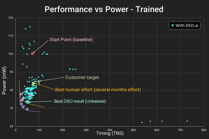
In this graph, we are plotting power against wire delay. The best way to look at this graph is to start at the labeled point at the top, which says Start Point.
- Start Point, where a basic quick layout is achieved
- Customer Target, what the customer would be happy with
- Best Human Effort, where humans get to after several months
- Best DSO result (untrained), where AI can get to in just 24 hours
All of the small blue points indicate one full AI sweep of placing the blocks in the design. Over 24 hours, the resources in this test showcase over 100 different results, with the machine learning algorithm understanding what goes where with each iteration. The end result is something well beyond what the customer requires, giving them a better product.
There is a fifth point here that isn't labeled, and that is the purple dots that represent even better results. This comes from the DSO algorithm on a pre-trained network specifically for this purpose. The benefit here is that in the right circumstances, even a better result can be achieved. But even then, an untrained network can get almost to that point as well, indicated by the best untrained DSO result.
Synopsys has already made some disclosures with customers, such as Samsung. Across four design projects, time to design optimization was reduced by 86%, from a month do days, using up to 80% fewer resources and often beating human-led design targets.

I did come away with several more questions that I hope Aart will address when the time comes.
Firstly I would like to address where the roadmaps lie in improving machine learning in chip design. It is one thing to make the algorithm that finds a potentially good result and then to scale it and produce 100s or 1000s of different configurations overnight, but is there an artificial maximum of what can be considered ‘best’, limited perhaps by the nature of the algorithm being used?
Second, Aart and I discussed Google’s competition with Go Master and 18-time world champion Lee Sedol, in which Google beat the world’s best Go player 4-1 in a board game that was considered impossible only five years prior for computers to come close to the best humans. In that competition, both the Google DeepMind AI and the human player made a ‘1-in-10000’ move, which is rare in an individual game, but one might argue is more likely to occur in human interactions. My question to Aart is whether machine learning for chip design will ever experience those 1-in-10000 moments, or rather in more technical terms, would the software still be able to find a best global minimum if it gets stuck in a local minimum over such a large (1 in 102500 combinations for chip design vs 1 in 10230 in Go) search space.
Third, and perhaps more importantly, is how applying machine learning at different levels of the design can violate those layers. Most modern processor design relies on specific ‘standard cells’ and pre-defined blocks – there will be situations where modified versions of those blocks might be better in some design scenarios when coupled close to different parts of the design. With all of these elements interacting with each other and having variable interaction effects, the complexity is in managing these interactions within the machine learning algorithms in a time-efficient way, but how these tradeoffs are made is still a point to prove.
In my recent interview with Jim Keller, I asked him if at one point we will see silicon design look unfathomable to even the best engineers – he said ‘Yeah, and it’s coming pretty fast’. It is one thing to talk holistically about what AI can bring to the world, but it’s another to have it working in action to improve semiconductor design and providing a fundamental benefit at the base level of all silicon. I’m looking forward to further disclosures on AI-accelerated silicon design from Synopsys, its competitors, and hopefully some insights from those that are using it to design their processors.


100 Comments
View All Comments
Everett F Sargent - Thursday, June 24, 2021 - link
After Moore’s Law: How Will We Know How Much Faster Computers Can Go?https://www.datacenterknowledge.com/supercomputers...
"In the middle of the last decade, the laws of physics finally had their say, denying transistors the ability to be shrunken any more than they already were. Betrayed by what one songwriter called “the flash of a neon light that split the night,” industries and economies everywhere began dumping the Law like an electorate dumping a losing candidate."
Read the whole thing even.
mode_13h - Thursday, June 24, 2021 - link
I think you're missing the point of the article. Don't get so hung up on the Moore's Law part that you miss the part about achieving real improvements that appear to be somewhat comparable to an additional node-shrink. That'd be a pretty big win, no?Everett F Sargent - Thursday, June 24, 2021 - link
You mean the part where AI or DL is not able to think outside the box? By definition, AI or DL is fundamentally limited by its own data driven boxes. Sure, you can extrapolate, but you can't extrapolate in all dimensions, thus you will never know the most efficient pathway, just A singular pathway.mode_13h - Friday, June 25, 2021 - link
Circuit layout is a highly-constrained problem. The AI is working in the same box as human designers or traditional automated layout tools. All the while, humans are defining the shape of the box, so to speak.It's a little hard to discuss by analogy or too much abstraction, but suffice to say I don's share your concern.
Everett F Sargent - Thursday, June 24, 2021 - link
AFTER MOORE'S LAWhttps://www.economist.com/technology-quarterly/201...
"After a glorious 50 years, Moore’s law—which states that computer power doubles every two years at the same cost—is running out of steam. Tim Cross asks what might replace it"
Circa 2016 even.
mode_13h - Friday, June 25, 2021 - link
> Circa 2016 even.What's even your point? People have been foretelling the end of Moore's Law since shortly after it was published! Jim Keller cited one of the more humorous takes on this phenomenon. I'm paraphrasing, since I can't seem to find the quote:
"Every 18 months, the number of people foretelling the end of Moore's Law doubles!"
Jim said that, in a matter of just a few weeks, his team at Intel identified room for a potential 50x increase in transistor density (presumably vs. their current 14 nm process, since that was in 2019). You can hear more of his thoughts on the subject, in this talk:
https://www.youtube.com/watch?v=oIG9ztQw2Gc
Calin - Thursday, June 24, 2021 - link
If this is an ad, it sells you what?I don't think you're in the target market for creating chip designs.
I appreciate it. Thank you Anandtech team :)
mode_13h - Wednesday, June 23, 2021 - link
I thought it was worth a read. As I hadn't heard about Google's experiment, this was all news to me.jlp2097 - Wednesday, June 23, 2021 - link
Agree that this is really ad-dy but then it is also very interesting and there is some added value from Ian. The AI enhancements will likely not be as easy or achieve as much as claimed, but even 1/3 of the claimed benefits would still be extremely valuable.Side note @Ian/@Ryan: the recent sponsored post by ARM was probably the first sponsored post that was actually interesting and relevant for anandtech readers. It was also the first time (at least for me) that comments were seemingly disabled. Was that on purpose/requested by ARM?
Ryan Smith - Wednesday, June 23, 2021 - link
"It was also the first time (at least for me) that comments were seemingly disabled. Was that on purpose/requested by ARM?"Advertisers can request to have comments disabled. That is a company (Future) policy.