TSMC Update: 2nm in Development, 3nm and 4nm on Track for 2022
by Anton Shilov on April 26, 2021 2:15 PM EST
For TSMC, being the world's largest foundry with nearly 500 customers has its peculiarities. On the one hand, the company can serve almost any client with almost any requirements. On the other hand, it has to stay ahead of everyone else both in terms of capacity and in terms of technology. As far as capacity is concerned, TSMC is unchallenged and is not going to be for years to come. As for fabrication technologies, TSMC has recently reiterated that it's confident that its N2, N3, and N4 processes will be available on time and will be more advanced than competing nodes.
Confidence
Early this year TSMC significantly boosted its 2021 CapEx budget to a $25 – $28 billion range, further increasing it to around $30 billion as a part of its three-year plan to spend $100 billion on manufacturing capacities and R&D.
About 80% of TSMC's $30 billion capital budget this year will be spent on expanding capacities for advanced technologies, such as 3nm, 4nm/5nm, and 6nm/7nm. Analysts from China Renaissance Securities believe that most of the money on advanced nodes will be used to expand TSMC's N5 capacity to 110,000 ~ 120,000 wafer starts per month (WSPM) by the end of the year. Meanwhile, TSMC said that 10% of its CapEx will be allocated for advanced packaging and mask making, whereas another 10% will be spent on specialty technologies (which includes tailored versions of mature nodes).
TMSC's the most recent CapEx hikes announcements were made after Intel announced its IDM 2.0 strategy (that involves in-house production, outsourcing, and foundry operations) and to a large degree reaffirms TMSC's confidence in both short-term and long-term future even ahead of intensified competition.
"As a leading pure-play foundry, TSMC has never been short on competition in our 30-plus-year history, yet we know how to compete," said C.C. Wei, president and CEO of TSMC, at a recent conference call with analysts and investors. "We will continue to focus on delivering technology leadership, manufacturing excellence, and earning our customers' trust. The last point, customers' trust, is fairly important because we do not have internal products that compete with customer."
| Advertised PPA Improvements of New Process Technologies Data announced during conference calls, events, press briefings and press releases |
|||||||||
| TSMC | |||||||||
| N7 vs 16FF+ |
N7 vs N10 |
N7P vs N7 |
N7+ vs N7 |
N5 vs N7 |
N5P vs N5 |
N4 vs N5 |
N3 vs N5 |
||
| Power | -60% | <-40% | -10% | -15% | -30% | -10% | lower | -25-30% | |
| Performance | +30% | ? | +7% | +10% | +15% | +5% | higher | +10-15% | |
| Logic Area Reduction % (Density) |
70% |
>37% |
- |
~17% |
0.55x -45% (1.8x) |
- |
? | 0.58x -42% (1.7x) |
|
| Volume Manufacturing |
2018 | 2018 |
2019 | Q2 2019 |
Q2 2020 | 2021 | 2022 | H2 2022 | |
N5 Gaining Customers
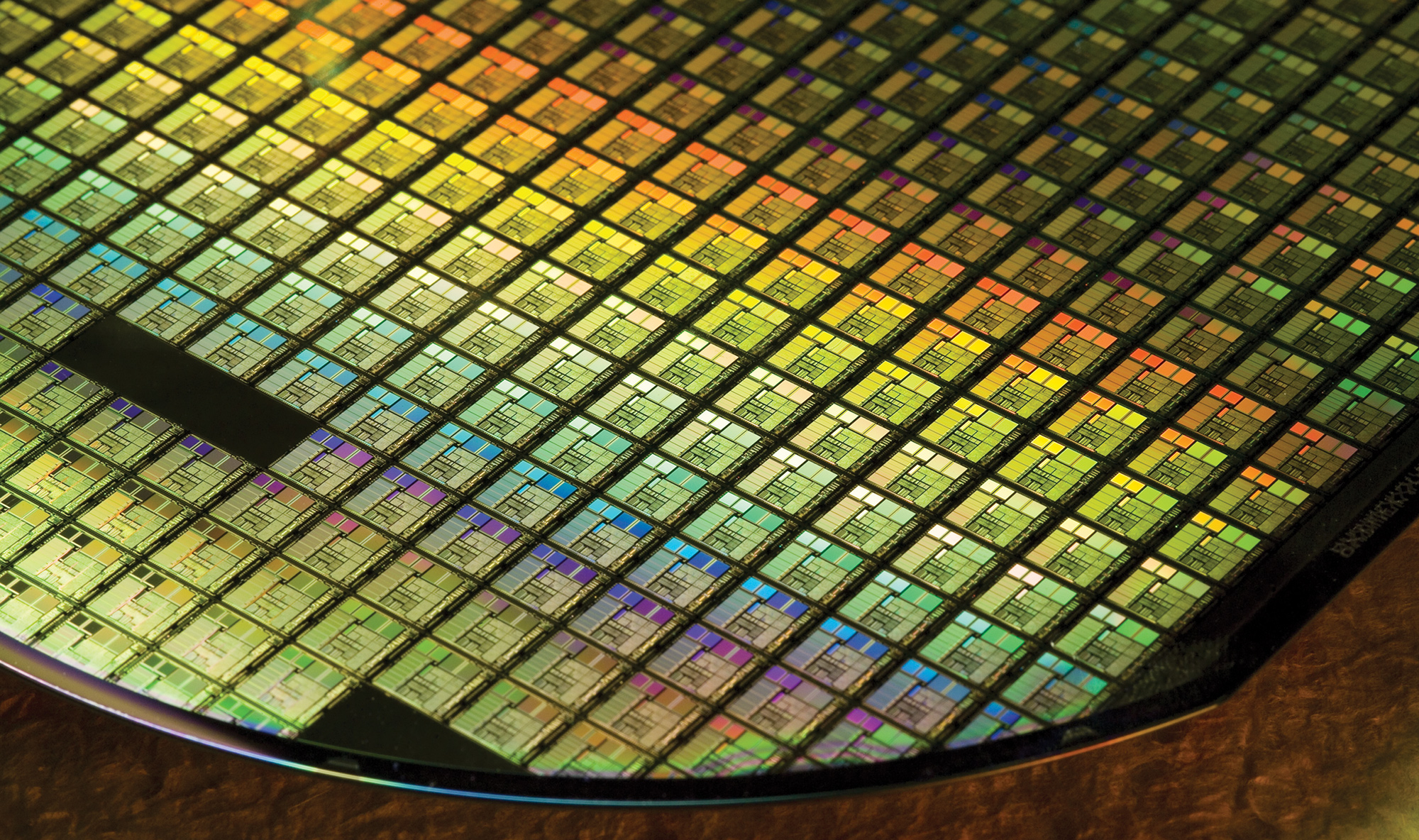
TSMC was the first company to start high volume manufacturing (HVM) of chips using its N5 (5 nm) process technology in mid-2020.
Initially, the node was used solely for TSMC's alpha customers — Apple and HiSilicon. Shipments to the latter ceased on September 14, which left all of the leading-edge capacity to Apple. By now, more customers are ready with their N5 designs, so the adoption of this node is growing. Meanwhile, TSMC says more customers are planning to use N5 family of technologies (including N5, N5P, and N4) than it expected just several months ago.
"N5 is already in its second year of volume production with yield better than our original plan," said Mr. Wei. N5 demand continues to be strong, driven by smartphone and HPC applications, and we expect N5 to contribute around 20% of our wafer revenue in 2021. […] In fact, we are seeing stronger engagement with more customers on 5 nm and 3 nm [versus 7 nm at similar stages]. The engagement is so strong that we have to really prepare the capacity for it."
For TSMC, HPC applications include many different types of products, including AI accelerators, CPUs, GPUs, FPGAs, NPUs, and video gaming SoCs, just to name a few. Since they're just a contract manufacturer, TSMC does not disclose what kinds of products it makes using one node or another (we do know that it builds the Apple A14 SoC for smartphones/tablets/STBs as well as the Apple M1 SoC for PCs and tablets), but the very fact that adoption of N5 is growing in the HPC segment is important.
"We expect demand for our N5 family to continue to grow in the next several years, driven by the robust demand for smartphone and HPC applications," the head of TSMC said. "We expect to see HPC, not only in the first wave, but in additional waves of demand to support our leading [N5] node in the future, actually."
It is not particularly surprising that TSMC's N5 is gaining market share among adopters of leading-edge technologies. Analysts from China Renaissance estimate that TSMC's N5 features a transistor density of around 170 million transistors per square millimeter (MTr/mm2), which if accurate, makes it the densest technology available today. By contrast, Samsung's Foundry's 5LPE can boast with about 125 MTr/mm2 ~130 MTr/mm2, whereas Intel's 10 nm features an approximately 100 MTr/mm2 density.
In the coming weeks TSMC is set to start making chips using a performance-enhanced version of its N5 technology called N5P that promises to increase frequencies by up to 5% or reduce power consumption by up to 10% (at the same complexity). The technology offers a seamless migration path for customers without requiring significant engineering resource investment or longer design cycle time, so anyone with an N5 design can use N5P instead. For example, early adopters of N5 could re-use their IP for their N5P chips.
N4: On Track for Next Year
TSMC's N5 family of technologies also includes evolutionary N4 process that will enter risk production later this year and will be used for mass production in 2022.
This technology is set to provide further PPA (power, performance, area) advantages over N5, but keep the same design rules, design infrastructure, SPICE simulation programs, and IPs. Meanwhile, since N4 further extends usage of EUV lithography tools, it also reduces mask counts, process steps, risks, and costs.
"N4 will leverage the strong foundation of N5 to further extend our 5 nm family," said Mr. Wei. "N4 is a straightforward migration from N5 with compatible design rules while providing further performance, power and density enhancement for the next wave of 5-nanometer products. N4 risk production is targeted for second half this year and volume production in 2022."
By the time N4 enters HVM in 2022, TSMC will have about two years of experience with N5 and three years of experience with EUV. So expectations are that yields will be high and the performance variability promises to be low.
But even as cutting-edge as N4 is slated to be, it's not going to be the most advanced fabrication technology that TSMC will offer next year.
N3: Due in H2 2022
In 2022, the world's largest contract maker of chips will roll out its brand-new N3 manufacturing process, which will keep using FinFET transistors, but is expected to offer the whole package of PPA improvements.
In particular, versus their current N5 process, TSMC's N3 promises to increase performance by 10% – 15% (at the same power and complexity) or reduce power consumption by 25% – 30% (at the same performance and complexity). All the while the new node will also improve transistor density by 1.1 ~ 1.7 times depending on the structures (1.1X for analog, 1.2X for SRAM, 1.7X for logic).
N3 will further increase the number of EUV layers, but will keep using DUV lithography. Also, since the technology keeps using FinFET, it will not require a new generation of electronic design automation (EDA) tools redesigned from scratch and development of all-new IPs, which might become a competitive advantage over Samsung Foundry's GAAFET/MBCFET-based 3GAE.
"N3 will be another full node stride from our N5 and will use FinFET transistor structure to deliver the best technology maturity, performance, and cost for our customers," said Mr. Wei. "Our N3 technology development is on track with good progress. We continue to see a much higher level of customer engagement for both HPC and smartphone applications at N3 as compared with N5 and N7."
In fact, TSMC's claims about growing customer engagement with N3 indirectly telegraphs its high expectations for N3.
"[N3] risk production is scheduled in 2021," said TSMC's CEO. "The volume production is targeted in second half of 2022. Our N3 technology will be the most advanced foundry technology in both PPA and transistor technology, when it is introduced. […] We are confident that both our [N5] and [N3] will be large and long-lasting nodes for TSMC."
Beyond N3
Gate-all-around FETs (GAAFETs) are still a part of TSMC's development roadmap. The company is expected to use a new kind of transistors with its 'post-N3' technology (presumably N2). In fact, the company is in path-finding mode for next generations of materials and transistor structures that will be used many years down the road.
"For advanced CMOS logic, TSMC’s 3nm and 2nm CMOS nodes are progressing nicely through the pipeline," the company said in its annual report recently. "In addition, TSMC's reinforced exploratory R&D work is focused on beyond-2nm node and on areas such as 3D transistors, new memory and low-R interconnect, which are on track to establish a solid foundation to feed into many technology platforms.
It is noteworthy that TSMC is expanding capacity for R&D operations at Fab 12, where N3, N2, and more advanced nodes are currently being researched and developed.
Summary
Overall, TSMC is confident that its "everyone's foundry" strategy will enable it grow further in terms of scale, market share, and sales. The company also expects to maintain its technology leadership going forward, which is pivotal for growth.
"For the full year of 2021, we now forecast […] foundry industry growth [at] about 16%," said Wendell Huang, CFO of TSMC, at a recent conference call with analysts and investors. "For TSMC, we are confident we can outperform the foundry revenue growth and grow by around 20% in 2021."
The company has a strong technology roadmap and it is set to continue introducing improved leading-edge nodes every year, thus offering its customers improvements at a predictable cadence.
TSMC knows how to compete against rivals with leading-edge nodes as well as makers of chips focused on specialty process technologies, so it does not see Intel Foundry Services (IFS) as an immediate threat especially because the blue giant is going primarily after leading-edge and advanced nodes.
Financial analysts generally share TSMC's optimism mainly because of the expectation that the company's N3 and N5 nodes are not going to have competitors offering similar transistor densities and wafer starts.
"Following Intel's announced foundry comeback in March, TSMC’s willingness to set a 3-year $100 billion CapEx/R&D investment plan, starting from 2021, indicates its confidence to widen its foundry leadership," Szeho Ng, an analyst with China Renaissance Securities. "We see TSMC’s strategic value rising with N3/N5: strong N5 tape-out activities from HPC/smartphone applications and more N3 client engagement vs N5/N7 at similar stages."


74 Comments
View All Comments
sharath.naik - Wednesday, May 5, 2021 - link
you mean intel on 10nm at best.. or most of it will still be on 14nm.. Intel will still be using that until they need to move.Oxford Guy - Monday, April 26, 2021 - link
What happened to SOI (silicon-on-insulator)? Did it die because IBM and Global Foundries focused on it? Or, is there an unavoidable technical impediment that makes it too uncompetitive? I suppose I should do a web search to answer the question.‘As far as capacity is concerned, TSMC is unchallenged and is not going to be for years to come.’
That’s an odd sentence.
juancn - Monday, April 26, 2021 - link
It's an odd sentence, but everyone else is so far behind, that it's probably true. Ramp up will take years for TSMC competitors, and that's to be where they are today, if they keep investing, the target moves further into the future.CiccioB - Monday, April 26, 2021 - link
It is 'odd' because a word is missing, not for its truthfulness:'As far as capacity is concerned, TSMC is unchallenged and is not going to be <b>[challenged]</b> for years to come.'
Probably it is what the intended meaning of the sentence was.
Santoval - Monday, April 26, 2021 - link
I also found it odd, but I think adding a second '--challenged' in the same sentence is problematic and kind of ugly. I think it would be cleaner to rephrase it as : 'As far as capacity is concerned, TSMC has no challenge and it is not going to have for years to come' or : 'As far as capacity is concerned, TSMC is unchallenged and that will remain the case for years to come'.BQP - Monday, April 26, 2021 - link
SOI going strong for the RF/Analog market. There is one size fits all in the IC industryCalin - Tuesday, April 27, 2021 - link
Silicon-on-insulator was a way to reduce power at the same frequency (lower capacitance hence lower current necessary to switch bits). Strained Silicon was a way to reduce resistance (same current needed to switch bits but lower heat losses).Both are useful, but they don't allow you to put more "bits" on the same area. And in the leading edge, he who has the most bits wins (as in, Intel's Rocket Lake has 8 cores on 14 nm whereas its equivalent Intel 10nm processor has 10 cores).
More "bits" (logic area) allows you to - for example - run a larger GPU at a lower speed for similar performance at lower power (or at higher performance and higher power). Or fit - in the same area - your smartphone processor but with more cache, more "AI" cores, more GPU cores, ....
Oxford Guy - Tuesday, April 27, 2021 - link
Yes, but is it somehow incompatible with the leading-edge stuff? High density hasn’t always been the most important factor. I remember reading about how the choice of choosing a high-density library vs. a high-performance library was not due to the former being simply better for all CPUs but because the CPUs (like Excavator as I recall) were specifically designed to be cheap + small lower-end parts.Having the density improvement from the node shrinkage does not seem to be the same problem thing as leveraging what you describe SOI’s benefit is. As you described them they seem to be complementary.
So, again I ask if there is something about SOI that’s an inherent impediment that keeps it from being used these days for the leading edge. Remember they back in 2011 Global Foundries was using SOI for its leading edge 32nm. There was also IBM as far as I know. So, what happened? Did finFET kill the tech by being incompatible and/or simply better —making SOI obsolete?
Oxford Guy - Tuesday, April 27, 2021 - link
‘the same problem thing’I didn’t write that. It was the groovy auto-defect in the phone. Anyway, the sentence should be intelligible. Just substitute ‘type’ for ‘problem’.
grant3 - Saturday, May 1, 2021 - link
According to the internets: SOI is used in some manufacturing but not much, because it's expensive.