The Snapdragon 888 vs The Exynos 2100: Cortex-X1 & 5nm - Who Does It Better?
by Andrei Frumusanu on February 8, 2021 3:00 AM EST- Posted in
- Mobile
- Samsung
- Qualcomm
- Smartphones
- SoCs
- Snapdragon 888
- Exynos 2100
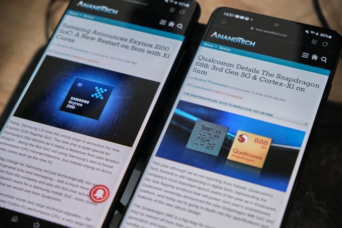
The new Galaxy S21 series of devices have been out commercially for a week now, and we’ve managed to get our hands on two Galaxy S21 Ultras – one with Qualcomm’s new Snapdragon 888 SoC, and one with Samsung’s new Exynos 2100 SoC. Both chipsets this year are more similar than ever, both now sporting similar CPU configurations, and both being produced on a new Samsung 5nm (5LPE) process node.
Ahead of our full device review of the Galaxy S21 Ultra (and the smaller Galaxy S21), today we’re focusing on the first test results of the new generation of SoCs, putting them through their paces, and pitting them against each other in the new 2021 competitive landscape.
The Snapdragon 888
| Qualcomm Snapdragon Flagship SoCs 2020-2021 | |||
| SoC | Snapdragon 865 |
Snapdragon 888 |
|
| CPU | 1x Cortex-A77 @ 2.84GHz 1x512KB pL2 3x Cortex-A77 @ 2.42GHz 3x256KB pL2 4x Cortex-A55 @ 1.80GHz 4x128KB pL2 4MB sL3 |
1x Cortex-X1 @ 2.84GHz 1x1024KB pL2 3x Cortex-A78 @ 2.42GHz 3x512KB pL2 4x Cortex-A55 @ 1.80GHz 4x128KB pL2 4MB sL3 |
|
| GPU | Adreno 650 @ 587 MHz | Adreno 660 @ 840MHz | |
| DSP / NPU | Hexagon 698 15 TOPS AI (Total CPU+GPU+HVX+Tensor) |
Hexagon 780 26 TOPS AI (Total CPU+GPU+HVX+Tensor) |
|
| Memory Controller |
4x 16-bit CH @ 2133MHz LPDDR4X / 33.4GB/s or @ 2750MHz LPDDR5 / 44.0GB/s 3MB system level cache |
4x 16-bit CH @ 3200MHz LPDDR5 / 51.2GB/s 3MB system level cache |
|
| ISP/Camera | Dual 14-bit Spectra 480 ISP 1x 200MP or 64MP with ZSL or 2x 25MP with ZSL 4K video & 64MP burst capture |
Triple 14-bit Spectra 580 ISP 1x 200MP or 84MP with ZSL or 64+25MP with ZSL or 3x 28MP with ZSL 4K video & 64MP burst capture |
|
| Encode/ Decode |
8K30 / 4K120 10-bit H.265 Dolby Vision, HDR10+, HDR10, HLG 720p960 infinite recording |
8K30 / 4K120 10-bit H.265 Dolby Vision, HDR10+, HDR10, HLG 720p960 infinite recording |
|
| Integrated Modem | none (Paired with external X55 only) (LTE Category 24/22) DL = 2500 Mbps 7x20MHz CA, 1024-QAM UL = 316 Mbps 3x20MHz CA, 256-QAM (5G NR Sub-6 + mmWave) DL = 7000 Mbps UL = 3000 Mbps |
X60 integrated (LTE Category 24/22) DL = 2500 Mbps 7x20MHz CA, 1024-QAM UL = 316 Mbps 3x20MHz CA, 256-QAM (5G NR Sub-6 + mmWave) DL = 7500 Mbps UL = 3000 Mbps |
|
| Mfc. Process | TSMC 7nm (N7P) |
Samsung 5nm (5LPE) |
|
Starting off with the new Snapdragon 888 SoC, Qualcomm’s new flagship model makes iterative steps this generation, with the biggest changes of the new design actually being in the form of the new Hexagon 780 accelerator, which fuses together traditional scalar and vector DSP operations with tensor execution engines within one single IP block.
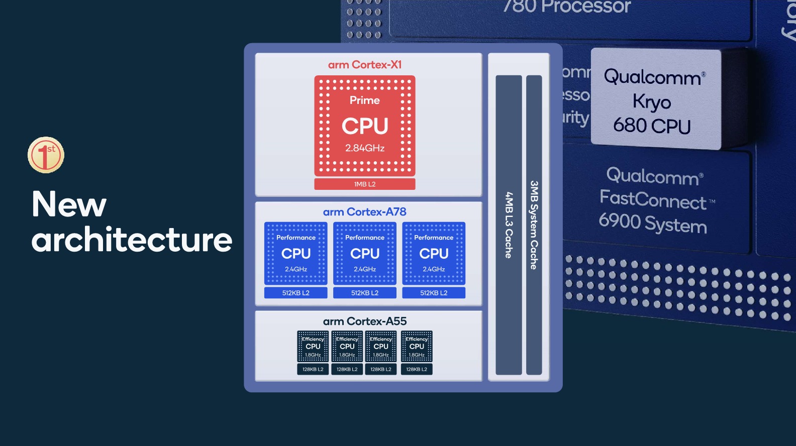
Of course, we’re also seeing upgrades elsewhere in the architecture, with the Snapdragon 888 being among the first SoCs to use Arm’s new Cortex-X1 CPU IP, promising large performance gains relative to last generation Cortex-A77 cores. The single X1 cores in the Snapdragon 888 clocks in at 2.84GHz – the same as the previous generation Snapdragon 865’s prime Cortex-A77 cores, and less than the 3.1GHz and 3.2GHz Snapdragon 865+ and recently announced Snapdragon 870 SoCs.
Alongside the X1, we find three Cortex-A78 cores at 2.42GHz, again the same clocks as the previous generation 865 SoCs, but this time around with double the L2 caches at 512KB.
The Cortex-A55 little cores remain identical this generation, clocking in at 1.8GHz.
Although we had been expecting 8MB L3 cache flagship SoCs this year, it does look like Qualcomm opted to remain at 4MB for this generation – but at least the company dons the X1 core with the maximum 1MB L2 cache configuration.
On the GPU side of things, Qualcomm’s new Adreno 660 GPU now clocks in up to a peak 840MHz – a whopping 43% higher frequency than the Snapdragon 865 GPU. The company’s performance claims here are also astonishing, promising a +35% boost in performance. We’ll have to see how this all ends up in terms of power consumption and long-term performance in the later dedicated GPU section.
What’s quite different for the Snapdragon 888 this year is that Qualcomm has moved from a TSMC N7P process node to Samsung’s new 5LPE node – the generally wildcard in this whole situation as we haven’t had any prior experience with this new 5nm node.
The Exynos 2100
| Samsung Exynos SoCs Specifications | ||
| SoC |
Exynos 990 |
Exynos 2100 |
| CPU | 2x Exynos M5 @ 2.73GHz 2MB sL2 3MB sL3 2x Cortex-A76 @ 2.50GHz 2x256KB pL2 4x Cortex-A55 @ 2.00GHz 4x64KB pL2 1MB sL3 |
1x Cortex-X1 @ 2.91GHz 1x512KB pL2 3x Cortex-A78 @ 2.81GHz 3x512KB pL2 4x Cortex-A55 @ 2.20GHz 4x64KB pL2 4MB sL3 |
| GPU | Mali G77MP11 @ 800 MHz | Mali G78MP14 @ 854 MHz |
| Memory Controller |
4x 16-bit CH @ 2750MHz LPDDR5 / 44.0GB/s 2MB System Cache |
4x 16-bit CH @ 3200MHz LPDDR5 / 51.2GB/s 6MB System Cache |
| ISP | Single: 108MP Dual: 24.8MP+24.8MP |
Single: 200MP Dual: 32MP+32MP (Up to quad simultaneous camera) |
| NPU | Dual NPU + DSP + CPU + GPU 15 TOPs |
Triple NPU + DSP + CPU + GPU 26 TOPs |
| Media | 8K30 & 4K120 encode & decode H.265/HEVC, H.264, VP9 |
8K30 & 4K120 encode & 8K60 decode H.265/HEVC, H.264, VP9 AV1 Decode |
| Modem | Exynos Modem External (LTE Category 24/22) DL = 3000 Mbps 8x20MHz CA, 1024-QAM UL = 422 Mbps ?x20MHz CA, 256-QAM (5G NR Sub-6) DL = 5100 Mbps (5G NR mmWave) DL = 7350 Mbps |
Exynos Modem Integrated (LTE Category 24/18) DL = 3000 Mbps 8x20MHz CA, 1024-QAM UL = 422 Mbps 4x20MHz CA, 256-QAM (5G NR Sub-6) DL = 5100 Mbps UL = 1920Mbps (5G NR mmWave) DL = 7350 Mbps UL = 3670 Mbps |
| Mfc. Process | Samsung 7nm (7LPP) |
Samsung 5nm (5LPE) |
On the Samsung LSI side of things, we find the brand-new Exynos 2100. Unlike the Snapdragon 888’s more incremental changes in terms of SoC design, the new Exynos is a rather large departure for Samsung’s SoC division as this is the first flagship design in many years that no longer uses Samsung’s own in-house CPU microarchitecture, but rather reverts back to using Arm Cortex cores, which in this case is also the new Cortex-X1 and Cortex-A78 cores.
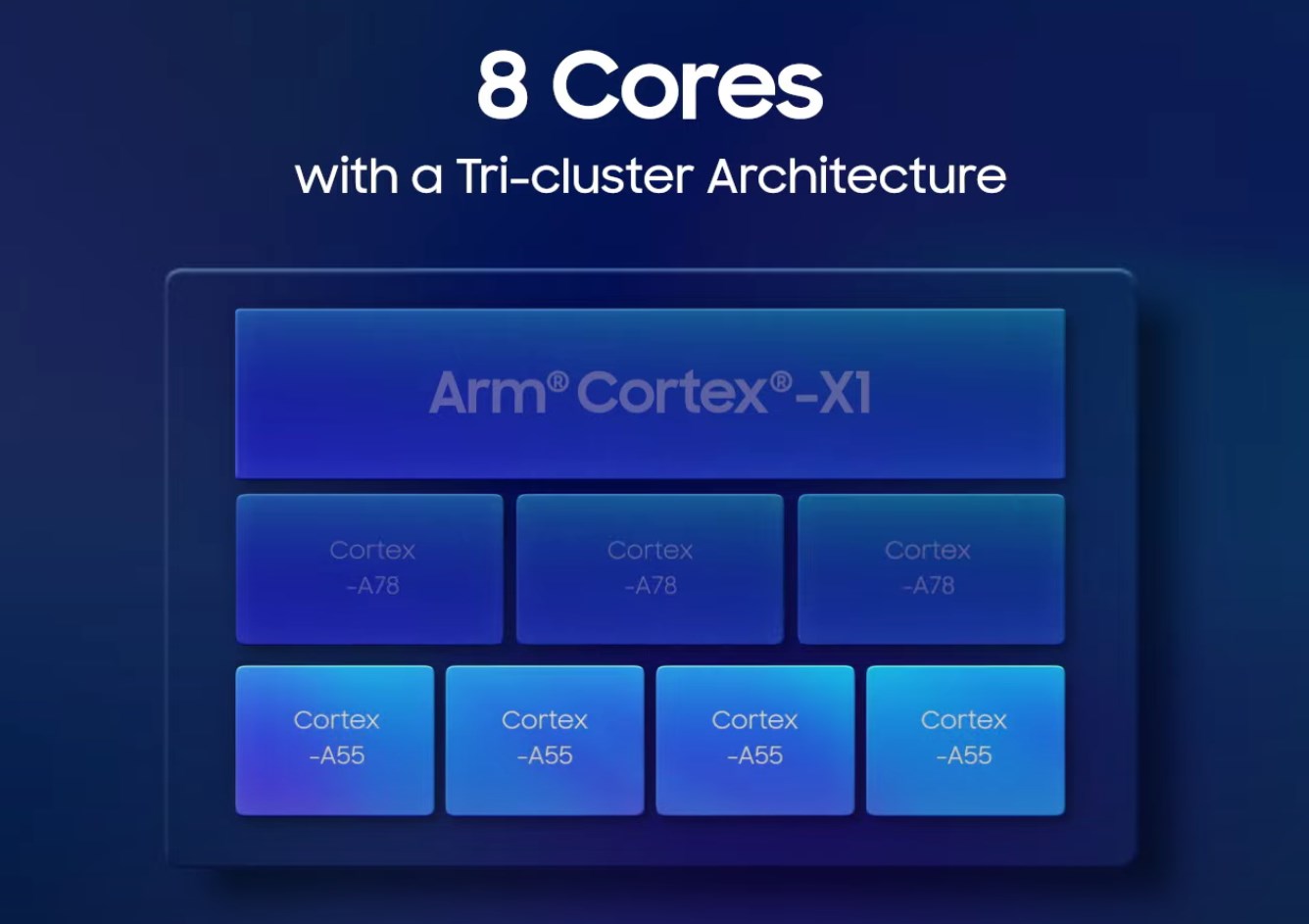
From a high-level, the CPU configuration of the Exynos 2100 looks nigh identical to that of the Snapdragon 888, as both are 1+3+4 designs with X1, A78 and A55 cores. The differences are in the details:
The X1 cores on the Exynos 2100 clock slightly higher at up to 2.91GHz, while the Cortex-A78 clock in significantly higher than the Snapdragon as they reach 2.81GHz. The Cortex-A55 cores are also quite aggressive in terms of frequency as they now reach 2.20GHz – so overall across the board higher clocks than the Snapdragon variant.
Where the Exynos isn’t as aggressive though is in its cache configurations. Most importantly, the X1 cores here only feature 512KB of L2 cache, which is a bit weird given the all-out-performance philosophy of the new CPU. The Cortex-A78s also see the usage of 512KB L2 caches, while the little A55 cores feature 64KB L2’s – less than the Snapdragon counterparts.
Much like the Snapdragon, the L3 cache also falls in at 4MB rather than the 8MB we would have hoped for this generation, however Samsung does surprise us with the usage of an estimated 6-8MB system level cache, up from the 2MB design in the Exynos 990.
On the GPU side of things, we see a Mali-G78MP14 at up to 854MHz. That’s 27% more cores and 6.7% higher frequency, and the company is also boasting massive performance gains as it touts a 40% generational improvement.
Let them fight
In today piece, we’ll be mostly focusing around CPU and GPU performance, as an especially interesting comparison will be to see how the two designs do against each other, given that they both now use Arm’s newest Cortex-X1 cores and both are sporting the same manufacturing node.
The GPU comparisons will also be interesting – and maybe quite controversial, as the results won’t be what many people will have been expecting.
While we would have liked to showcase AI performance of the two SoCs – unfortunately the software situation on the Galaxy S21’s right now means that neither SoC are fully taking advantage of their new accelerators, so that’s a topic to revisit in a few months’ time once the proper frameworks have been updated by Samsung.


123 Comments
View All Comments
mohamad.zand - Thursday, June 17, 2021 - link
Hi , thank you for your explanationDo you know how many transistors Snapdragon 888 and Exynos 2100 are?
It is not written anywhere
Spunjji - Thursday, February 11, 2021 - link
I'm not an expert by any means, but I think Samsung's biggest problem was always optimisation - they use lots of die area for computing resources but the memory interfaces aren't optimised well enough to feed the beast, and they kept trying to push clocks higher to compensate.The handy car analogy would be:
Samsung - Dodge Viper. More cubes! More noise! More fuel! Grrr.
Qualcomm / ARM - Honda Civic. Gets you there. Efficient and compact.
Apple - Bugatti Veyron. Big engine, but well-engineered. Everything absolutely *sings*.
Shorty_ - Monday, February 15, 2021 - link
you're right but you also don't really touch why Apple can do that and X86 designs can't. The issue is that uOP decoding on x86 is *awfully* slow and inefficient on power.This was explained to me as follows:
Variable-length instructions are an utter nightmare to work with. I'll try to explain with regular words how a decoder handles variable length. Here's all the instructions coming in:
x86: addmatrixdogchewspout
ARM: dogcatputnetgotfin
Now, ARM is fixed length (3-letters only), so if I'm decoding them, I just add a space between every 3 letters.
ARM: dogcatputnetgotfin
ARM decoded: dog cat put net got fin
done. Now I can re-order them in a huge buffer, avoid dependencies, and fill my execution ports on the backend.
x86 is variable length, This means I cannot reliably figure out where the spaces should go. so I have to try all of them and then throw out what doesn't work.
Look at how much more work there is to do.
x86: addmatrixdogchewspoutreading frame 1 (n=3): addmatrixdogchewspout
Partially decoded ops: add, , dog, , ,
reading frame 2 (n=4): matrixchewspout
Partially decoded ops: add, ,dog, chew, ,
reading frame 3 (n=5): matrixspout
Partially decoded ops: add, ,dog, chew, spout,
reading frame 4 (n=6): matrix
Partially decoded ops: add, matrix, dog, chew, spout,
Fully Expanded Micro Ops: add, ma1, ma2, ma3, ma4, dog, ch1, ch2, ch3, sp1, sp2, sp3
This is why most x86 cores only have a 3-4 wide frontend. Those decoders are massive, and extremely energy intensive. They cost a decent bit of transistor budget and a lot of thermal budget even at idle. And they have to process all the different lengths and then unpack them, like I showed above with "regular" words. They have excellent throughput because they expand instructions into a ton of micro-ops... BUT that expansion is inconsistent, and hilariously inefficient.
This is why x86/64 cores require SMT for the best overall throughput -- the timing differences create plenty of room for other stuff to be executed while waiting on large instructions to expand. And with this example... we only stepped up to 6-byte instructions. x86 is 1-15 bytes so imagine how much longer the example would have been.
Apple doesn't bother with SMT on their ARM core design, and instead goes for a massive reorder buffer, and only presents a single logical core to the programmer, because their 8-wide design can efficiently unpack instructions, and fit them in a massive 630μop reorder buffer, and fill the backend easily achieving high occupancy, even at low clock speeds. Effectively, a reorder buffer, if it's big enough, is better than SMT, because SMT requires programmer awareness / programmer effort, and not everything is parallelizable.
Karim Braija - Saturday, February 20, 2021 - link
Je suis pas sur si le benchmark SPENCint2006 est vraiment fiable, en plus je pense que ça fait longtemps que ce benchmark est là depuis un moment et je pense qu'il n'a plus bonne fiabilité, ce sont de nouveaux processeurs puissant. Donc je pense que ce n'est pas très fiable et qu'il ne dit pas des choses précises. Je pense que faut pas que vous croyez ce benchmark à 100%.serendip - Monday, February 8, 2021 - link
"Looking at all these results, it suddenly makes sense as to why Qualcomm launched another bin/refresh of the Snapdragon 865 in the form of the Snapdragon 870."So this means Qualcomm is hedging its bets by having two flagship chips on separate TSMC and Samsung processes? Hopefully the situation will improve once X1 cores get built on TSMC 5nm and there's more experience with integrating X1 + A78. All this also makes SD888 phones a bit pointless if you already have an SD865 device.
Bluetooth - Monday, February 8, 2021 - link
Why would they skimp on the cache. Was neural engine or something else with higher priority getting silicon?Kangal - Tuesday, February 9, 2021 - link
I think Samsung was rushing, and its usually easier to stamp out something that's smaller (cache takes alot of silicon estate). Why they rushed was due to a switch from their M-cores to the X-core, and also internalising the 5G-radio.Here's the weird part, I actually think this time their Mongoose Cores would be competitive. Unlike Andrei, I estimated the Cortex-X1 was going to be a load of crap, and seems I was right. Having node parity with Qualcomm, the immature implementation that is the X1, and the further refined Mongoose core... it would've meant they would be quite competitive (better/same/worse) but that's not saying much after looking at Apple.
How do I figure?
The Mongoose core was a Cortex A57 alternative which was competitive against Cortex A72 cores. So it started as midcore (Cortex A72) and evolved into a highcore implementation as early as 2019 with the S9 when they began to get really wide, really fast, really hot/thirsty. Those are great for a Large Tablet or Ultrabook, but not good properties for a smaller handheld.
There was a precedence for this, in the overclocked QSD 845 SoCs, 855+, and the subpar QSD 865 implementation. Heck, it goes all the way back to 2016 when MediaTek was designing 2+4+4 core chipsets (and they failed miserably as you would imagine). I think when consumers buy these, companies send orders, fabs design them, etc... they always forget about the software. This is what separates Apple from Qualcomm, and Qualcomm from the rest. You can either brute-force your way to the top, or try to do things more cost/thermal efficiently.
Andrei Frumusanu - Tuesday, February 9, 2021 - link
> Unlike Andrei, I estimated the Cortex-X1 was going to be a load of crap, and seems I was right.The X1 *is* great, and far better than Samsung's custom cores.
Kangal - Wednesday, February 10, 2021 - link
First of all, apologies for sounding crass.Also, you're a professional in this field, I'm merely an enthusiast (aka Armchair Expert) take what I say with a grain of salt. So if you correct me, I stand corrected.
Nevertheless, I'm very unimpressed by big cores: Mongoose M5, to a lesser extent the Cortex-X1, and to a much Much much lesser extent the Firestorm. I do not think the X1 is great. Remember, the "middle cores" still haven't hit their limits, so it makes little sense to go even thirstier/hotter. Even if the power and thermal issues weren't so dire with these big-cores, the performance difference between the middle cores vs big cores is negligible, also there is no applications that are optimised/demand the big cores. Apple's big-core implementation is much more optimised, they're smarter about thermals, and the performance delta between it and the middle-cores is substantial, hence why their implementation works and why it favours compared to the X1/M5.
I can see a future for big-cores. Yet, I think it might involve killing the little-cores (A53/A55), and replacing it with a general purpose cores that will be almost as efficient yet be able to perform much better to act as middle-cores. Otherwise latency is always going to be an issue when shifting work from one core to another then another. I suspect the Cortex-X2 will right many wrongs of the X1, combined with a node jump, it should hopefully be a solid platform. Maybe similar to the 20nm-Cortex A57 versus the 16nm-Cortex A72 evolution we saw back in 2016. The vendors have little freedom when it comes to implementing the X1 cores, and I suspect things will ease up for X2, which could mean operating at reasonable levels.
So even with the current (and future) drawbacks of big-cores, I think they could be a good addition for several reasons: application-specific optimisations, external dock. We might get a DeX implementation that's native to Android/AOSP, and combined that with an external dock that provides higher power delivery AND adequate active-cooling. I can see that as a boon for content creators and entertainment consumers alike. My eye is on emulation performance, perhaps this brute-force can help stabilise the weak Switch and PS2 emulation currently on Android (WiiU next?).
iphonebestgamephone - Monday, February 15, 2021 - link
The improvement with the 888 in damonps2 and eggns are quite good. Check some vids on youtube.