Qualcomm Details The Snapdragon 888: 3rd Gen 5G & Cortex-X1 on 5nm
by Andrei Frumusanu on December 2, 2020 10:00 AM EST- Posted in
- Mobile
- Qualcomm
- Smartphones
- SoCs
- 5G
- Cortex A78
- Cortex X1
- Snapdragon 888
This year although we’re not reporting from Hawaii, Qualcomm’s Tech Summit is still happening in digital form, representing the company’s most important launch event of the year as it showcases the new flagship products that will power next year’s smartphones. Qualcomm yesterday announced the new Snapdragon 888 SoC and platform, and today we’re going in-depth into the specifications and features of the new silicon design.
The Snapdragon 888 is a big leap for Qualcomm, so much so that they’ve veered off from their usual naming scheme increments this generation and even skipped the 87x series altogether. The 888 number is not there only for marketing purposes as it represents fortune and luck in Chinese, but the new SoC has some substantial generational changes that sets it apart from the usual yearly improvements of past.
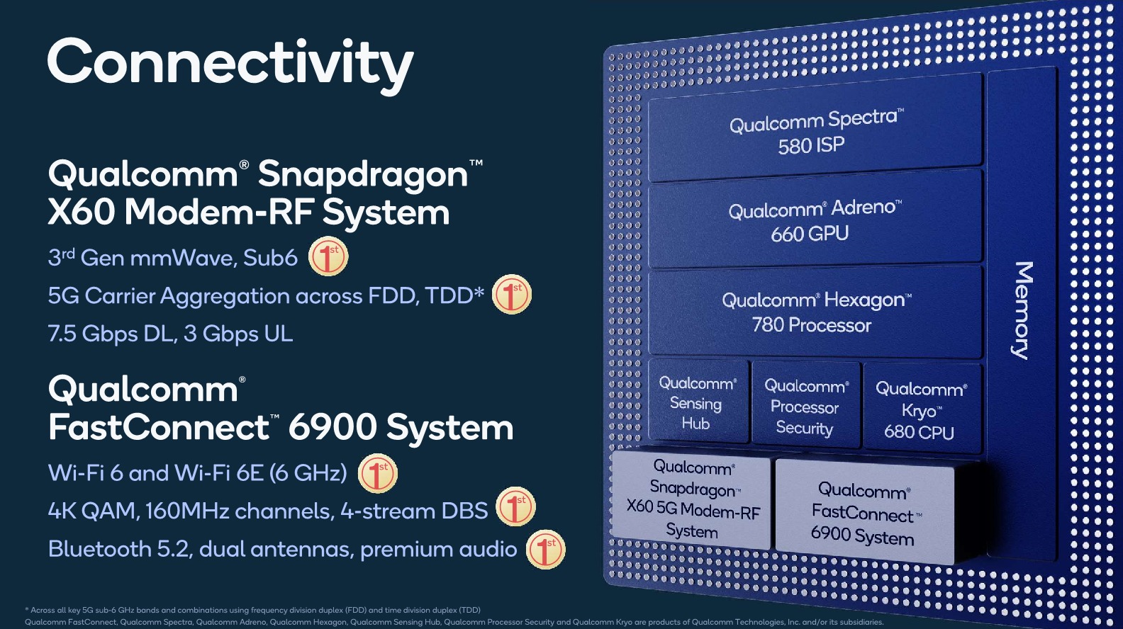
Featuring the first ever implementation of a Cortex-X1 CPU core as its performance engine, new Cortex-A78 cores for efficiency, a massive +35% boost in GPU performance, a totally new DSP/NPU IP redesigned from the ground up, triple camera ISPs, integrated 5G modem, all manufactured on a new 5nm process node, the new Snapdragon 888 touches and updates almost every part of the SoC design with significant uplifts in performance and capabilities. There is a lot to cover, so let’s go over the details piece by piece:
| Qualcomm Snapdragon Flagship SoCs 2020-2021 | |||
| SoC | Snapdragon 865 |
Snapdragon 888 |
|
| CPU | 1x Cortex-A77 @ 2.84GHz 1x512KB pL2 3x Cortex-A77 @ 2.42GHz 3x256KB pL2 4x Cortex-A55 @ 1.80GHz 4x128KB pL2 4MB sL3 |
1x Cortex-X1 @ 2.84GHz 1x1024KB pL2 3x Cortex-A78 @ 2.42GHz 3x512KB pL2 4x Cortex-A55 @ 1.80GHz 4x128KB pL2 4MB sL3 |
|
| GPU | Adreno 650 @ 587 MHz |
Adreno 660 @ ?MHz +35% perf |
|
| DSP / NPU | Hexagon 698 15 TOPS AI (Total CPU+GPU+HVX+Tensor) |
Hexagon 780 26 TOPS AI (Total CPU+GPU+HVX+Tensor) |
|
| Memory Controller |
4x 16-bit CH @ 2133MHz LPDDR4X / 33.4GB/s or @ 2750MHz LPDDR5 / 44.0GB/s 3MB system level cache |
4x 16-bit CH @ 3200MHz LPDDR5 / 51.2GB/s 3MB system level cache |
|
| ISP/Camera | Dual 14-bit Spectra 480 ISP 1x 200MP or 64MP with ZSL or 2x 25MP with ZSL 4K video & 64MP burst capture |
Triple 14-bit Spectra 580 ISP 1x 200MP or 84MP with ZSL or 64+25MP with ZSL or 3x 28MP with ZSL 4K video & 64MP burst capture |
|
| Encode/ Decode |
8K30 / 4K120 10-bit H.265 Dolby Vision, HDR10+, HDR10, HLG 720p960 infinite recording |
8K30 / 4K120 10-bit H.265 Dolby Vision, HDR10+, HDR10, HLG 720p960 infinite recording |
|
| Integrated Modem | none (Paired with external X55 only) (LTE Category 24/22) DL = 2500 Mbps 7x20MHz CA, 1024-QAM UL = 316 Mbps 3x20MHz CA, 256-QAM (5G NR Sub-6 + mmWave) DL = 7000 Mbps UL = 3000 Mbps |
X60 integrated (LTE Category 24/22) DL = 2500 Mbps 7x20MHz CA, 1024-QAM UL = 316 Mbps 3x20MHz CA, 256-QAM (5G NR Sub-6 + mmWave) DL = 7500 Mbps UL = 3000 Mbps |
|
| Mfc. Process | TSMC 7nm (N7P) |
Samsung 5nm (5LPE) |
|
Re-integration of the 5G modem into the SoC
The most important aspect for this year’s design is the fact that Qualcomm is going back to an fully integrated modem design, contrasting last year’s surprising choice of the Snapdragon 865 not containing any modem at all and having instead to rely on the external X55 modem.
Last year’s rationale of going with an external modem was said to have been a practical one, stemming from the fact that 5G was still in its early stages and that many vendors had to make a lot of design efforts when designing their new handsets for 5G. A external 5G modem such as the X55 helped the 5G transition as it was available to vendors earlier than the Snapdragon 865 SoC itself, allowing them to design their RF systems before having access to the newest SoC.
This year, the market has evolved and is more mature, and Qualcomm chose to re-integrate the modem into the same silicon die as the SoC. The new X60 modem subsystem is the company’s 3rd generation 5G design and brings new capabilities in terms of carrier aggregation and 5G frequency band interoperability.
The platform’s reabsorption of the modem into the SoC die should signify better power efficiency, lower platform cost as well as lower PCB complexity for smartphone vendors.
2020 certainly was the year that 5G became a mainstream feature amongst device vendors, with essentially everybody adopting the new standard into their flagship and even mid-range devices. The new X60 modem will further mature the 5G experience by providing more flexibility to network operators in terms of frequency band support.
mmWave in particular has been a rather contentious aspect of 5G in 2020 as network deployments has been rather scarce and limited to US cities, with users reporting spotty reception with a larger impact on battery life. mmWave network expansion is progressing at a steady pace, and Qualcomm states that the new Snapdragon 888 platform completely solves the power efficiency concerns around mmWave usage. Hopefully 2021 will be the year where mmWave becomes a lot more useful and practical for users.
Whilst mmWave is expected to still be relatively niche for the vast majority of users, Sub-6GHz will be the workhorse of 5G, and here we’re seeing rapid expansion and deployments in countries all over the world. The new X60’s modem capability of allowing for carrier aggregation between FDD (Frequency Division Duplex, dedicated frequency bands between upload & download) and TDD (Time Division Duplex, upload & download in the same frequency band) means that network carriers will be able to mix and match more available Sub-6GHz spectrum together for even greater bandwidth.
DSS, or dynamic spectrum sharing, is also going to be a key technology enabling network operators to migrate existing LTE frequency bands to 5G NR dynamically based on the organic LTE/5G user demand – meaning that the frequency spectrum doesn’t need to be segregated for each technology, thus allowing more actual usable bandwidth for both types of users in the first few years and consumers switch over to 5G-capable handsets.
Manufactured on Samsung 5nm / 5LPE
The new Snapdragon 888 is making the transition from 7nm to 5nm, but the new design doesn’t merely make a process shift, it’s also making a foundry shift. After being with TSMC for the 7nm generations of the Snapdragon 855 and Snapdragon 865, Qualcomm is now switching back to Samsung Foundry and their new 5LPE process node for the new Snapdragon 888.
Qualcomm in recent years had been dual-sourcing from both TSMC and Samsung depending on the SoC design and product range, but in the high-end flagship SoC segment the company seems to have always chosen the technologically superior node as it had larger implications for the competitiveness of those parts. N7 and N7P were clear winning choices for the S855 and S865 as Samsung’s own 7LPP process was kind of late, and didn’t seem to be quite as good as TSMC’s variants. Qualcomm notably still used the 7LPP node on this year’s Snapdragon 765 SoC which has seen a lot of success in the premium range of device designs, however we had noted earlier in the year that it didn’t appear to be nearly as efficient as the TSMC-manufactured flagship SoC.
This year’s choice of switching back to a Samsung process for the flagship SoC seems to be a vote of confidence in the new process node- as otherwise Qualcomm likely wouldn’t have made the switch. Versus 7LPP, Samsung promises a 20% decrease in power consumption at the same performance, or a 10% increase in performance at the same power, together with a +-20% area reduction. How these figures will translate over to practical improvements for the new Snapdragon 888 remains to be seen.
Another rationale for the foundry switch could be manufacturing capacity. As Apple is eating up a lot of TSMC’s early 5nm capacity with the A14 and M1, Qualcomm probably saw Samsung’s 5LPE as the safer choice this year as the new Snapdragon 888 may be manufactured in the new dedicated EUV V1 line at Hwaesong.
It’ll be hard to gauge the process node switch for this generation as we don’t expect to see a similar design on TSMC’s 5nm node – unless MediaTek somehow has a new Cortex-X1 SoC in the pipeline for next year.
Powered by Cortex-X1 and Cortex-A78 CPUs
The Snapdragon 888 is the first publicly announced SoC powered by the new Cortex-X1 and Cortex-A78 CPU IPs by Arm. The Cortex-X1 in particular is the first of a new generation of CPU IP by Arm that focuses on maximising performance at the cost of lesser power efficiency, while the Cortex-A78 being the same-generation design but which still prioritises a balance between performance, power and area.
The new X1 core, based on Arm’s numbers, promised a +30% uplift in IPC over the last generation Cortex-A77 which was also deployed in the Snapdragon 865. Qualcomm advertises a 25% uplift over the Snapdragon 865, but that’s likely due to a few configuration differences on the part of the new Snapdragon 888 compared to Arm’s own internal figures.
The S888 continues to use a 1+3+4 CPU setup this generation, with the big difference being that instead of using the same CPU IP with a different physical implementation, the new 1+3 big cores are actually of different microarchitectures.
The “prime” performance core as Qualcomm likes to call it is the new Cortex-X1 design, clocking in at the same 2.84GHz as the Snapdragon 865’s prime core. The new core is configured with the maximum 1MB of L2 cache.
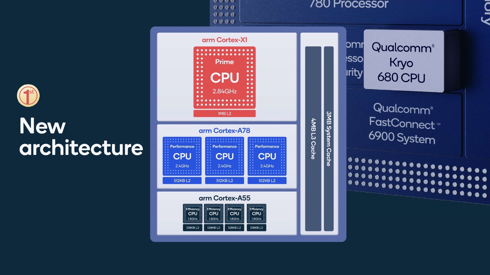
What stood out for me during our briefing of the new chip is that the clock frequency of the new design isn’t all very aggressive at all. Qualcomm’s 25% performance boost is in comparison to the vanilla Snapdragon 865 which also came at the same frequency. Compared to the Snapdragon 865+ which clocks in at 3.09GHz, this performance advantage should reduce to only 13%, which is less impressive.
Qualcomm’s 25% generational boost is also less than Arm’s advertised 30% as the new S888 continues to use a 4MB L3 cache for the CPU cluster, versus Arm’s envisioned 8MB configuration for a high-end 5nm SoC with the new X1 cores. Qualcomm explained to us that this was simply a balance between cost, implementation effort, and diminishing returns of a higher cache configuration design.
What this all means is that there’s a high chance that the Snapdragon 888 won’t be holding the Android CPU performance crown next year if Samsung’s next-gen Exynos SoC is even a little more aggressive in terms of clocks or cache configurations.
The high-performance X1 cores is joined by three Cortex-A78 cores clocking in at up to 2.4GHz, serving as the every-day workhorse CPUs for most computational tasks. In terms of cache, the new cores see their L2 doubled up from 256KB to 512KB.
One aspect I was interested in finding out is whether the new design still continues Qualcomm choice of fitting all the big cores together on a single voltage plane, which oddly enough, also seems to be the case for the new Snapdragon 888. This means that while the X1 and A78 cores can run at different frequencies, they’re all powered by the minimum voltage of either operating frequency at any one time. Qualcomm explains that this is again a practical choice surrounding the design complexity of the power delivery system, particularly mentioning that the X1 core can take advantage of the increased capacitance available from the larger shared power plane. Whilst this has worked well for the Snapdragon 855 and 865, I wonder that given the new X1 core’s increased performance and dynamic range, if the company isn’t leaving further performance or efficiency gains on the table for the sake of lower power delivery design cost. It’ll be interesting to see how other SoC vendors tackle their X1 implementations.
Finally, the big cores are again accompanied by four Cortex-A55 cores. This year the company yet again clocks them at 1.8GHz, which makes this the 4th generation SoC with an essentially identical configuration of little cores, which is a bit disappointing. Qualcomm can’t do much here as there’s simply a need for a new little core CPU IP, something which we’ll hopefully see released next year in 2021 for 2022 SoCs.


123 Comments
View All Comments
lmcd - Wednesday, December 2, 2020 - link
820 was absolutely a disaster. Its errata list was too great for Windows kernel support, likely at the ISA implementation, and likely deeply-rooted enough to justify dropping the entire endeavor.Silver5urfer - Wednesday, December 2, 2020 - link
How is Windows Kernel coming into the picture ?It was about the Android performance and 64Bit compat due to Apple's move first and 810's ultimate disaster which even killed HTC entirely. 820 processor was very fast and still holds up, just like 805 but the latter was 32bit, One can see comparison of that with Apple's A9.
Entire endeavor was dropped because there's no need. Why do you think Qcomm develops a lot of the Radio and etc and tons of R&D ? Patents. That's what Qcomm is all about and they tried that with Centriq. But ARM on DC market is a dead end, so many years of articles here on AT and STH, so far no one is there on that side the only option which was showing some metric of performance that too for small loads is Graviton2. Only when there's a need then these companies push, which is money. Apple does it because they want to hold that position to leverage their pricing justification of the iPhone. Looking at any Android top flagship vs iPhone real world application performance tests and gaming loads it shows why there is no need for Qcomm to push, they push where there is money, GPU and NPU, ISP, Radio RF.
techconc - Thursday, December 3, 2020 - link
Qualcomm and Samsung had different problems with their CPU designs. Qualcomm had a pretty competitive design. Their problem was getting blind-sided by the A7 with 64bit. They didn't have a 64bit design in their pipeline and had to abandon their own work and go back to ARM reference designs just to have something remotely competitive.Samsung found out the hard way that chip design isn't easy. Making a more powerful chip is one thing, but being energy efficient (and powerful) is quite another thing. They eventually scuttled their custom chip hopes as well.
That leaves ARM. ARM will design what their customers want. It's not clear that customers are complaining to ARM that they want more powerful cores. Maybe the X1 is a step in that direction. However, we can see lots of cost cutting examples in the SD888, so it's not clear that there is an appetite for an Apple like design for Android based SoC vendors.
ZolaIII - Thursday, December 3, 2020 - link
A55 is not inferior, it's still the best in order A core ARM ever made. The so called Apple little core's are simple OoO core's inferior but closest to compare to A73. Problem is ARM never made a newer incarnation of A73 suitable for DynamIQ clusters. They did make Neoverse E1 and A65 which both thanks to SMT aren't exactly suitable for mobile phones and we didn't see any of their actual silicone implementations.I don't see a L3 victim cache as the way to go as it's limiting in many aspects. Faster RAM & bigger L2 cache should be a way to go.
Apple just makes your wallet cry.
AntonErtl - Thursday, December 3, 2020 - link
The A75 is derived from the A73 (3-wide instead of 2-wide), and AFAIK supports DynamIQ. And looking at Andrei's M4 review, the A75 appears to be almost as efficient as the A55 at the A55's lowest voltage, and more efficient if the A55 has to ramp up the voltage (long before it reaches the performance of the A75 at its lowest voltage).Wilco1 - Friday, December 4, 2020 - link
Even better would be a low clocked and slightly cut-down Cortex-A76. According to AnandTech at lower frequencies it is more efficient than Cortex-A55 while being much faster. It has a larger area of course, but you could cut it down a bit, and 4 little cores seems a bit overkill, 1 or 2 would be more than enough for background tasks.Irish910 - Monday, December 14, 2020 - link
Apple efficiency cores have much better performance and power efficiency versus other chips with a similar design. (High perf/low perf).It’s amazing to see what Apple has achieved since the A9 year over year just dominating performance while keeping power efficiency. It’s not even close with Apple GPUs.
You’ll probably squabble that Metal is more optimized than OpenGL.
When it comes to chip designs, whether you like apple or not, they are the best.
patel21 - Wednesday, December 2, 2020 - link
Was Samsung going to use AMD GPU this year ? It they do, I can see them wearing the Android Performance Crown easily.darkich - Wednesday, December 2, 2020 - link
I don't understand why they just don't ditch the A55 cores and use two underclocked A78s instead.The A78 is the most power efficient CPU on the planet at under 2GHz!..yes I'm not forgetting the Icestorm from Apple.
1X1 + 3A78 +2A78 should be optimal according to me..what am I missing?!
lmcd - Wednesday, December 2, 2020 - link
Die size considerations.What you're really identifying here is that the paragraph at the end of page 1 is extremely damning. Qualcomm isn't good enough with intricate work on multiple voltage planes to deliver a the best possible SoC.