Rambus Develops HBM2E Controller & PHY: 3.2 Gbps, 1024-Bit Bus
by Anton Shilov on March 6, 2020 3:00 PM EST
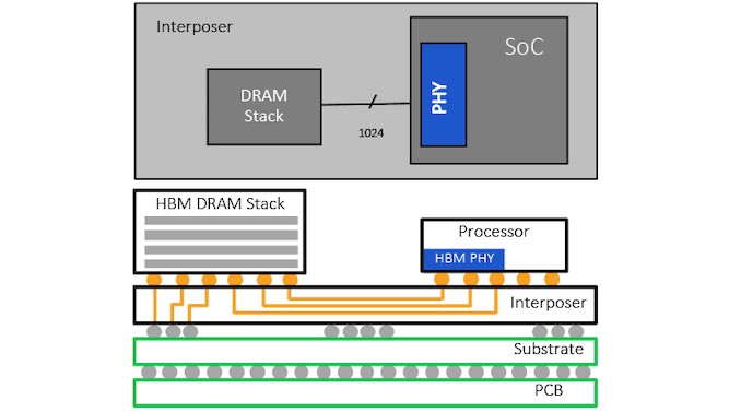
The latest enhancements to the HBM2 standard will clearly be appreciated by developers of memory bandwidth-hungry ASICs, however in order to add support of HBM2E to their designs, they are also going to need an appropriate controller as well as physical interface. For many companies developing of such IP in-house does not make financial sense, so Rambus has designed a highly-integrated HBM2E solution for licensing.
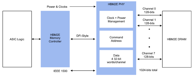
The HBM2E standard supports 12-Hi DRAM stacks as well as memory devices of up to 16 Gbps, thus enabling to build up to 24 GB stacks using a 1024-bit bus. At the same time, the new specification officially supports data rates of up to 3.2 Gbps, which results in 409.6 GB/s bandwidth per stack. Rambus’s HBM2E solution includes a controller that can work with 12-Hi KGSDs (known good stack dies) as well as a verified 1024-bit PHY that supports speeds of up to 3.2 Gbps.
The Rambus HBM2E controller core (originally developed by Northwest Logic) is DFI 3.1 compatible (with appropriate extensions) and supports AXI, OCP or proprietary interfaces to connect to integrator logic. Meanwhile, the controller also supports Look-Ahead command processing (a standard way to trim latencies) as well as channel densities of up to 24 Gb.
Licensees of Rambus’s HBM2E solution will get everything they need to integrate it into their designs, including source code of the controller (in a bid to synthesize it for a particular process technology) as well as fully-characterized hard macros (GDSII) of the interface. Alternatively, engineers from Rambus can help integrate the HBM2E IP support for a fee.
Related Reading:
- JEDEC Updates HBM2 Memory Standard To 3.2 Gbps; Samsung's Flashbolt Memory Nears Production
- GlobalFoundries and SiFive to Design HBM2E Implementation on 12LP/12LP+
- Samsung Develops 12-Layer 3D TSV DRAM: Up to 24 GB HBM2
- SK Hynix Announces 3.6 Gbps HBM2E Memory For 2020: 1.8 TB/sec For Next-Gen Accelerators
- Samsung HBM2E ‘Flashbolt’ Memory for GPUs: 16 GB Per Stack, 3.2 Gbps
Source: Rambus


42 Comments
View All Comments
webdoctors - Sunday, March 8, 2020 - link
That's not entirely accurate. When you license a commercial IP block design from someone, its verified and tested. Its something tangible that is production quality. Its not just a block diagram and a patent. Otherwise what's to stop someone from printing out all the papers from ASPLOS/MICRO/ISCA and filing them all at the patent office and hoping it passes under the radar of the authors and selling it to 3rd parties as a "design" folks can license.When you get a block from Syopsys or Cadence or other 3rd party IP design companies its usually pretty mature and maybe even taped out on a test chip to ensure it works.
tldr Avoid Rambus unless you want to spend more on lawyers than engineers
UltraWide - Monday, March 9, 2020 - link
Thank you for this! It's nice to have some facts once in a while!Yojimbo - Friday, March 13, 2020 - link
What facts? The fact that Rambus hasn't sued anybody in something like 20 years? Why do you his assertions that make no sense to be "facts"? You believe that Rambus are forcing people to buy their PHYs?Yojimbo - Friday, March 13, 2020 - link
Please source me where you get the idea that Rambus's IP blocks are not verified and tested whereas others are. And even if so, it's not relevant, because if Rambus's blocks are not verified or tested then that is perfectly OK with their customers who choose them. I believe what I said was entirely accurate and what you said is just nonsense.balle - Thursday, March 26, 2020 - link
You might want to step into DesignCon and see a working demo of this technology that is tested, verified and is being used by multiple customersDeeDee - Sunday, May 31, 2020 - link
So you're saying that Rambus doesn't collaborate, verify and test?<<Samsung and eSilicon Taped Out 14nm Network Processor with Rambus 28G SerDes Solution>>
https://news.samsung.com/global/samsung-and-esilic...
DeeDee - Sunday, May 31, 2020 - link
You're saying that Rambus doesn't do tape outs?<<Rambus Announces Tapeout of GDDR6 Memory PHY on TSMC 7nm Process Technology
Leading IP to support TSMC’s customers with AI, HPC, automotive and networking applications
SUNNYVALE and SANTA CLARA, Calif. – Jan. 30, 2019 >>
https://www.rambus.com/rambus-announces-tapeout-of...
DeeDee - Sunday, May 31, 2020 - link
No tape outs? Why do you comment without understanding what you're commenting about?Rambus Tapes Out 112G XSR SerDes PHY on Leading-edge 7nm Process
Highlights:
Provides critical building block to deliver data for next-generation data center, networking, high-performance computing (HPC), artificial intelligence (AI) and machine learning (ML) applications
Delivers superior power, performance and area (PPA) for extra short reach (XSR) links with innovative architecture designed for leading-edge 7nm process node
Expands SerDes PHY portfolio for 112G OIF-CEI industry standard
SUNNYVALE, Calif. – Sep. 25, 2019
https://www.rambus.com/rambus-tapes-out-112g-xsr-s...
DeeDee - Sunday, May 31, 2020 - link
Yojimbo, thank you for your informed and intelligent comment.I would think that individuals reading about technology would have high enough
IQs to make informed and well thought out comments. But too bad that isn't the
case in some instances. Some bring up old and misinformed biases that they
just can't grow out of!
ravyne - Sunday, March 8, 2020 - link
Appears to be a typo in the second paragraph, it says memory devices of up to 16Gbps, but I think you mean to say 16Gb.