Analyzing Intel’s Discrete Xe-HPC Graphics Disclosure: Ponte Vecchio, Rambo Cache, and Gelato
by Dr. Ian Cutress on December 24, 2019 9:30 AM EST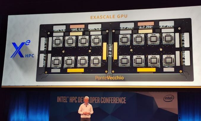
It has been a couple of weeks since Intel formally provided some high-level detail on its new discrete graphics strategy. The reason for the announcements and disclosures centered around Intel’s contract with the Department of Energy to build Aurora, an exascale supercomputer at the Argonne National Laboratory. The DoE and Argonne want developers clued into the hardware early, so when the supercomputer is deployed it can be used with as little ‘learning time’ as possible. This means Intel had to flesh out some of its strategy, as well as lift the lid on its first announced discrete GPU product. Only time will tell if it’s a bridge too far, or over troubled water, but today we know it as Ponte Vecchio.
Intel On Discrete Graphics: A Quick Recap
While Intel has had a graphics portfolio for a couple of decades, those graphics solutions have been limited to embedded graphics and integrated graphics solutions. There was a slight attempt to move into the graphics space and play with the big boys, with the Intel i740, however that was a long time ago. Intel’s current graphics architecture, called ‘Gen’, is currently in use in hundreds of millions of mobile devices, and is present in a substantial number of desktop processors, even if a discrete GPU is being used instead.
Intel has had high hopes for the graphics space before. Known as ‘Larrabee’, Intel attempted to engineer what was essentially x86 based graphics: using wide vector engines based on the same code path as Intel CPUs, the idea was to provide high-end graphics performance with the ease of programming in standard CPU code. While that product did actually run a number of graphics demos over the years, the hardware ended up being put to use in the high-performance computing market, where some developers saw the use of five-dozen 512-bit wide vector units absolutely fantastic for their simulations. This was the birth of AVX-512, which has lived on and now in Intel’s Xeon Scalable CPUs as well as consumer-grade Ice Lake laptop processors. The product that ‘Larrabee’ ended up as, Xeon Phi, scored a number of supercomputer wins and originally the Xeon Phi ‘Knights Hill’ product was destined to be put into Aurora in 2020. However the Xeon Phi program only lasted a few generations, with the final ‘Knights Mill’ hardware not being widely deployed and subsequently put to pasture.
Fast forward several years, and some management adjustments, and Intel has decided once again to enter the big graphics market. This time they’re going with something more conventional, something that looks more like a traditional graphics design. While the project started somewhere around three years ago, the big announcement that Intel was serious was when the company hired Raja Koduri, AMD’s Chief Graphics Architect in December 2017, and then Jim Keller, renowned SoC Guru. Raja Koduri’s title, Chief Architect, and his two decade of experience in building graphics solutions at AMD and Apple showcased how serious Intel was with this.
Since December 2017, Intel hasn’t said much about its new graphics plans. Under Ari Rauch, notable marketing figures and analysts were hired to be part of the team. Intel disclosed at its Architecture Day in December 2018 that the graphics solutions it would offer would be a full top-to-bottom implementation, covering low power integrated graphics all the way to the high-end. At the time Intel stated there would be two main GPU microarchitectures, all building from the ‘Xe’ architecture. Xe is meant to stand for ‘eXascale for Everyone’ (rather than x^2.718), with the marketing message that Intel wants to put high-end performance and efficiency anywhere it can.
As part of HPC DevCon, and Intel’s announcement with the DoE/Argonne, the veil was lifted, and we were told very slightly more than just the high level information. We were lucky enough to speak with Raja Koduri in a worldwide exclusive for the event, as his first official 1-on-1 interview since he joined Intel. It is worth a read and gives his perspective on a lot of ideas, as well as some of the decisions he has made.

This article is going to dive into Intel’s HPC DevCon disclosures about their graphics strategy. Here we are going to cover some of the blurb about Intel’s big plans, the new ‘third’ microarchitecture in Xe called Xe-HPC, the new GPU product ‘Ponte Vecchio’, Intel’s new Memory Fabric, a breakdown of the oneAPI software stack as presented, and what all this means for the rest of Intel’s graphics platform.
Exascale for Everyone
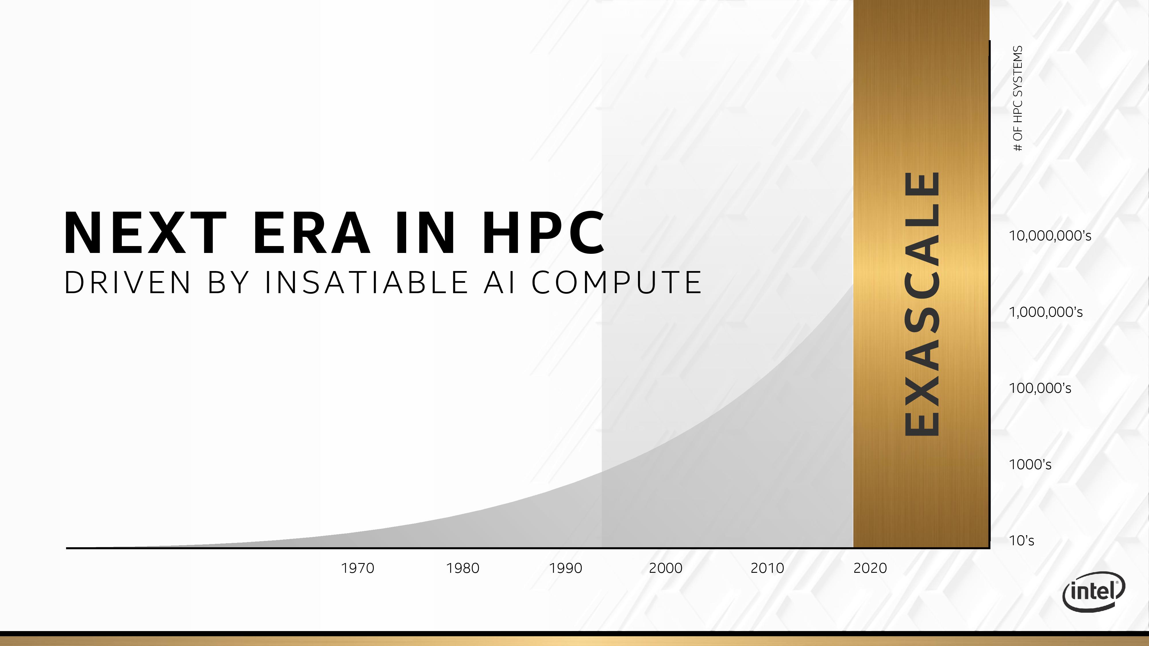
Intel says that it is hard not to notice the ‘insatiable’ demand for faster, more power efficient compute. Not only that, but certain people want that compute at scale, specifically at ‘exascale’. (It was disclosed at a high-performance supercomputing event, after all). For 2020 and beyond, Intel has designated this the ‘Exascale’ era in computing, where no amount of compute is good enough for leading edge research.
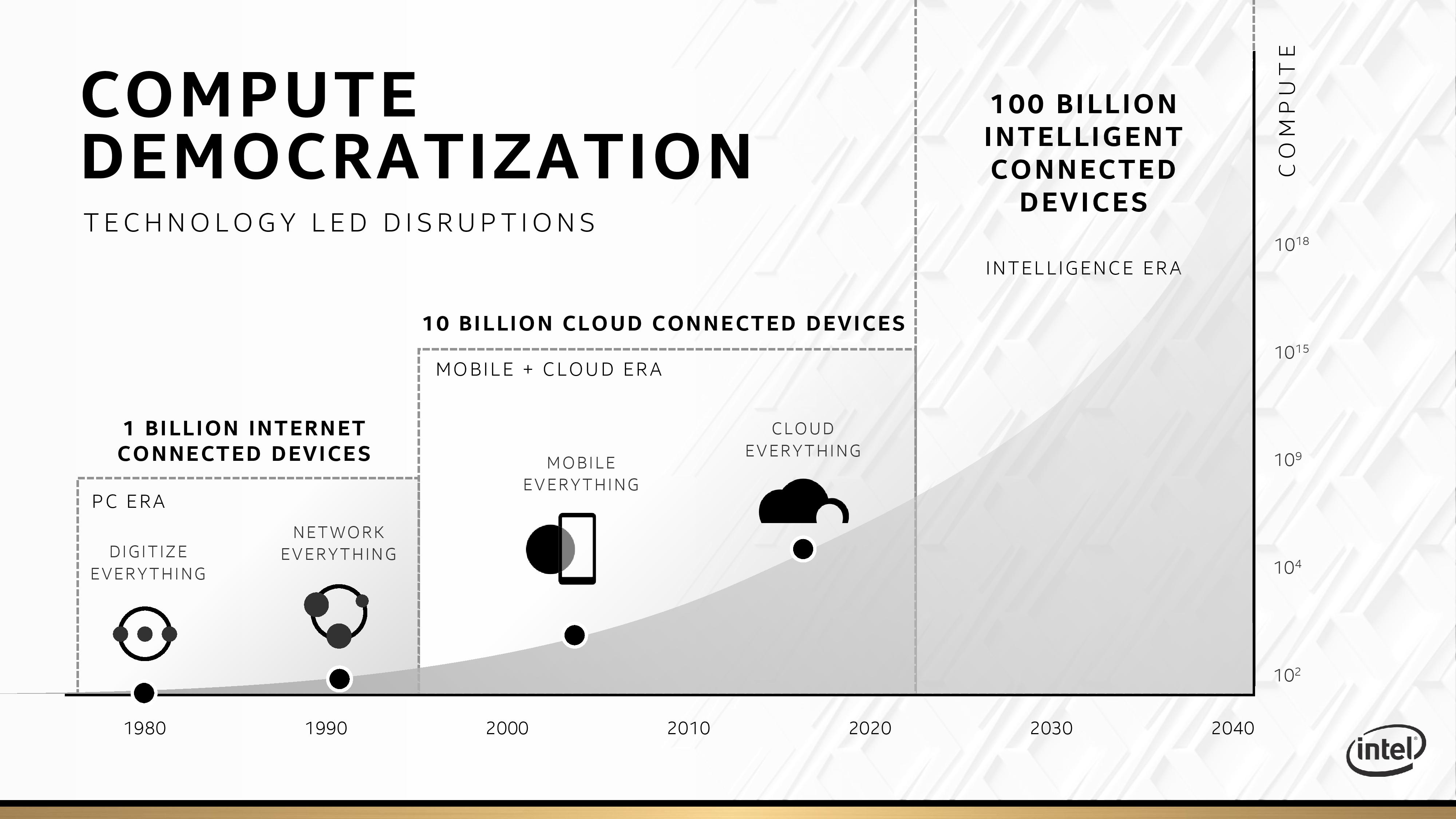
On top of this, Intel points to the number of connected devices in the market. A few years ago analysts were predicting 50 B IoT devices by 2020-2023, and in this presentation Intel is saying that by mid-2020 and beyond, there will be 100 billion devices that require some form of intelligent compute. The move to implementing AI, both in terms of training and inference, means that performance and computational ability have to be ubiquitous: beyond the network, beyond the mobile device, beyond the cloud. This is Intel’s vision of where the market is going to go.
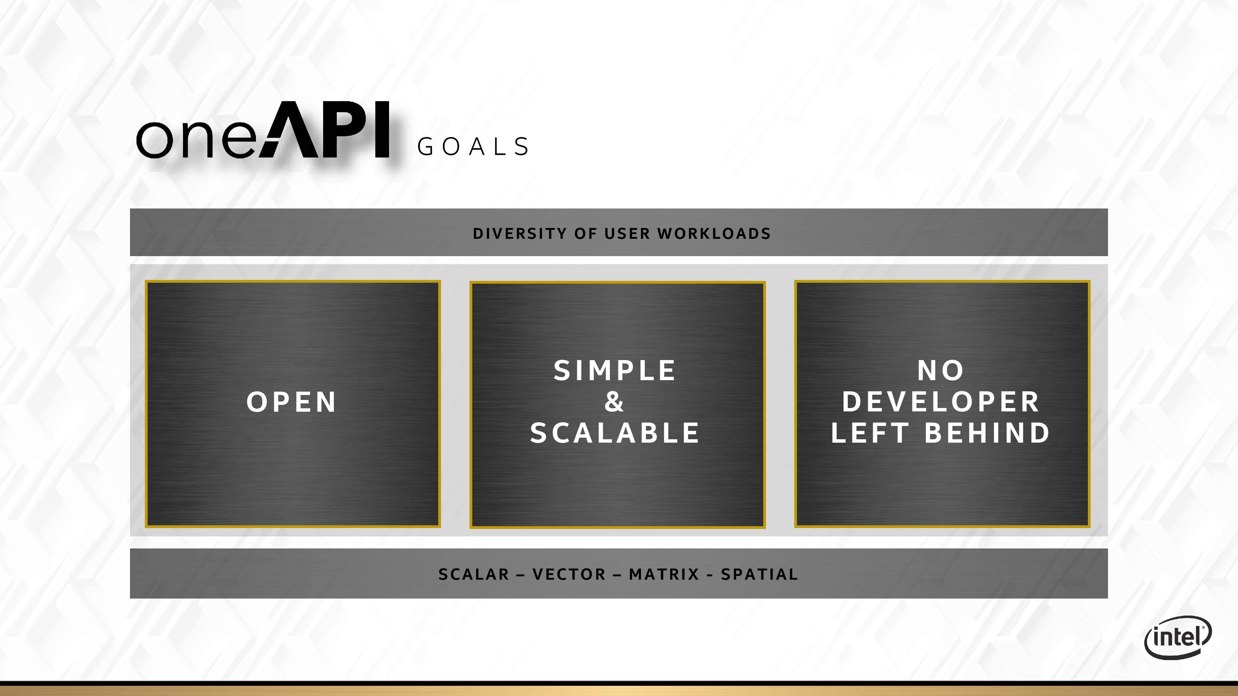
Intel splits this up into four specific categories of compute: Scalar, Vector, Matrix, and Spatial. This is certainly one blub part of the presentation I can say I agree with, having done high-performance programming in a previous career. Scalar compute, is the standard day-to-day compute that most systems run on. Vector compute is moving to parallel instructions, while Matrix compute is the talking point of the moment, with things like tensor cores and AI chips all working to optimize matrix throughput. The other part of the equation is spatial compute, which is derived from the FPGA market: for sparse compute that is complex and can be optimized with its own non-standard compute engine, then an FPGA solves it. Obviously Intel’s goal here is to cover each of these four corners with dedicated hardware: CPU for Scalar, GPU for Vector, AI for Matrix, and FPGA for Spatial.

One of the issues with hardware, as you move from CPU to FPGA, is that it becomes more and more specialized. A CPU for example can do Scalar, Vector, Matrix, and Spatial, in a pinch. It’s not going to be much good at some of those, and the power efficiency might be poor, but it can at least do them, as a launching point onto other things. With GPU, AI, and FPGA, these hardware specializations come with different amounts of complexity and a higher barrier to entry, but for those that can harness the hardware, large speed-ups are possible. In an effort to make compute more ubiquitous, Intel is pushing its oneAPI plan with a singular focal resource for all four types of hardware. More on this later.
Intel’s Xe architecture will be the underpinning for all of its GPU hardware. It represents a new fundamental redesign from its current graphics architecture, called ‘Gen’, and pulls in what the company has learned from products such as Larrabee/Xeon Phi, Atom, Core, Gen, and even Itanium (!). Intel officially disclosed that it has its first Xe silicon back from the fabs, and has performed power cycling and basic functionality testing with it, keen to promote that it is an actual thing.
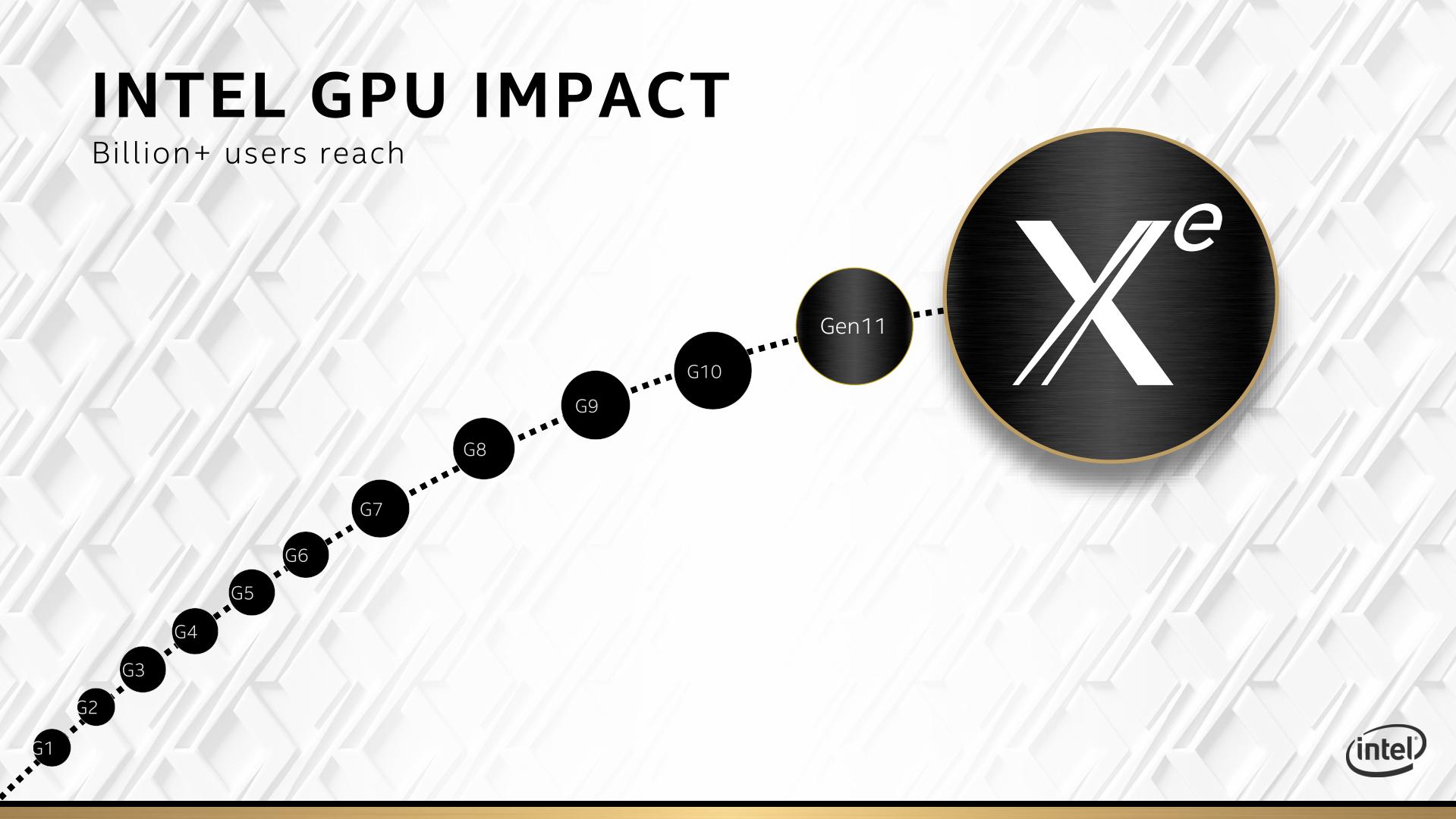
So far the latest ‘Gen’ graphics we have seen is the Gen11 graphics solution, which is on the newest Ice Lake consumer notebook processors. These are out in the market, ready to buy today, and feature performance 2x over the previous Gen9/Gen9.5 designs. (I should point out that Gen10 shipped in Cannon Lake but was disabled: this is the only graph ever where I’ve seen Intel officially acknowledge the existence of Gen10 graphics.) We have seen diagrams, either potentially from Intel or elsewhere, showing ‘Gen12’. It would appear that ‘Gen12’ was just a holding name for Xe, and doesn’t actually exist as an iteration of Gen. When we asked Raja Koduri about the future of Gen, he said that all the Gen developers are now working on Xe. There are still graphics updates to Gen, but the software developers that can be transferred to Xe have been already.
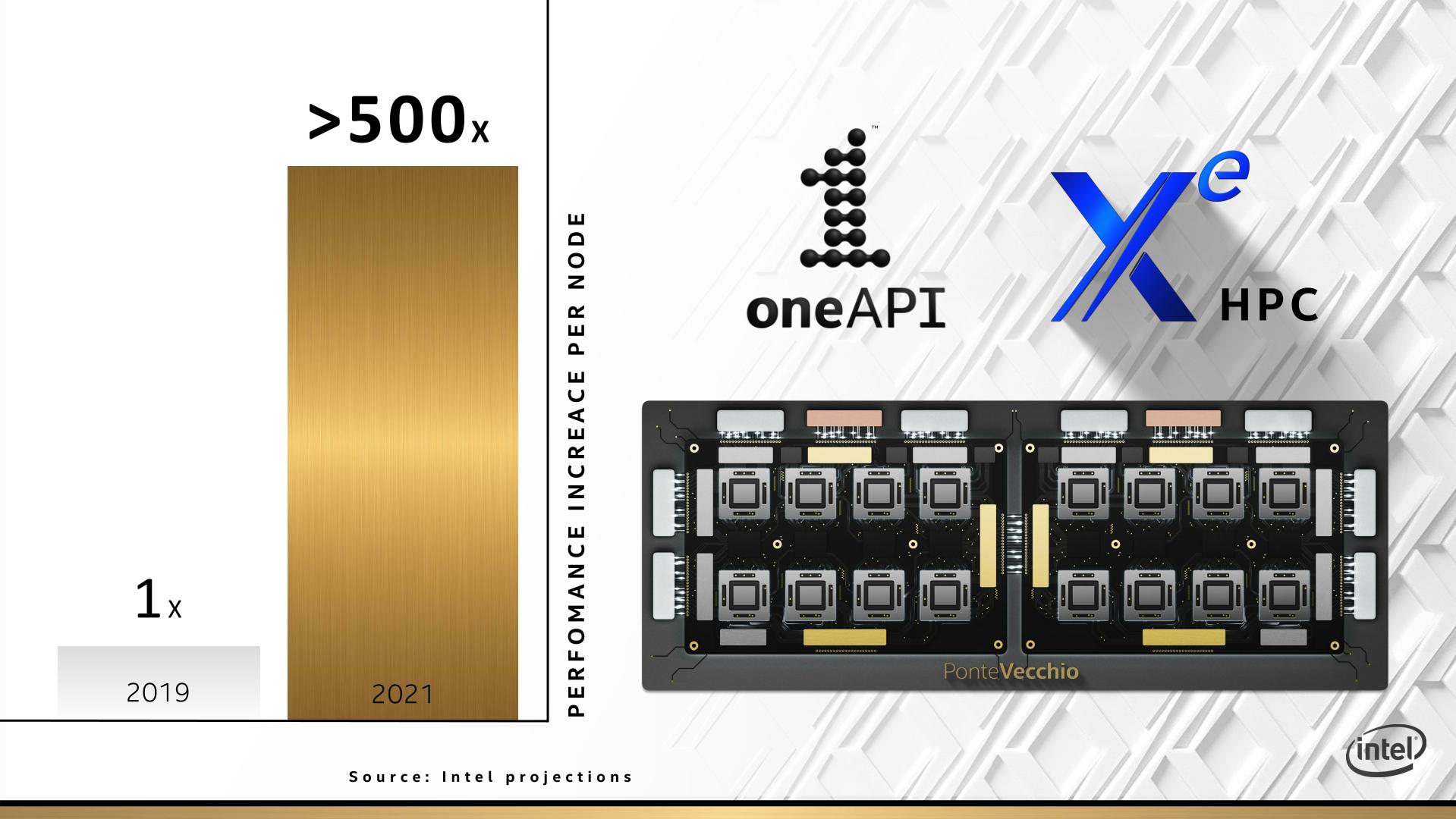
If you’re only going to read one thing today, then I want to skip ahead to Raja’s final slide of what he presented at HPC DevCon. Putting a quite ambitious goal in front of the audience, it showed that Intel wants to be able to provide a 500x in performance per server node by the end of 2021 compared to the per-node performance in 2019.
Now it is worth noting that this goal wasn’t specifically nailed down: are we comparing vector code running in scalar mode on a single 6-core Xeon Bronze in 2019 to an optimized dual-socket with six Xe GPUs in 2021? 500x is a big bet to make, so I hope Intel is ready.
In the next few pages, we’ll cover Xe, Ponte Vecchio, oneAPI, and Aurora.


47 Comments
View All Comments
Spunjji - Friday, December 27, 2019 - link
They were even worse on the notebook side of things. They were happy to sling dual-core + HT CPUs as "i7" processors until AMD announced the 2500U / 2700U; suddenly Intel came up with a "new" 15W Kaby Lake R CPU that looked suspiciously like a TDP-limited Kaby Lake, which itself was just a voltage-tweaked Skylake on an improved 14nm process.Any interested hobbyists can observe the extent of the truth in this by taking a notebook with a 45W quad-core Skylake CPU, undervolting it by 100-125mV (the vast majority will do this) and dropping in a TDP limit. The barely perceptible change in performance that results is truly something to behold. My own tweaked 6700HQ averages a 22W TDP under load just from the undervolt.
extide - Monday, December 30, 2019 - link
Yeah just described what a mobile CPU is, why are you surprised?JayNor - Wednesday, January 1, 2020 - link
I think if you asked Intel, they'd say ADAS, FPGAs and Optane are still very exciting programs for them, and probably already making money on ADAS and FPGAs.Intel shipped 88 million LTE modems for iphones this year. How many LTE modems did AMD deliver?
Korguz - Thursday, January 2, 2020 - link
sources ????Spunjji - Friday, December 27, 2019 - link
Depends whether you're focusing entirely on the CPU side of their business or making a more general assessment. Generally speaking, they've burned money on all sorts of unsuccessful projects (see: Atom cores in phones and tablets, their 4G modem projects).Even on the CPU side they had their fair share of struggles prior to the 10nm-induced disasters. Ivy Bridge was a weak and somewhat cheapened follow-up to the absolute blockbuster that was Sandy, while Broadwell arrived late and barely showed its face at all on the desktop due to early struggles with 14nm. These things didn't have larger effects because AMD and their foundry competitors were performing so terribly at the time, but they were missteps nonetheless.
Spunjji - Friday, December 27, 2019 - link
Agreed re: worryingly light on technical details. I'm sure it all feels very real to the engineers working on it, but from an end-user perspective this is still very much a marketing exercise.Sychonut - Wednesday, December 25, 2019 - link
Raja "The Wood Elf" Koduri better not let his mouth write a check his ass can't cash.Spunjji - Friday, December 27, 2019 - link
Those who observed the Vega launch know he has no such compunctions :DGreenReaper - Thursday, December 26, 2019 - link
Hmm. That HPC block diagram . . . where have I seen it before . . .https://www.resetera.com/threads/how-would-a-ryzen...
peevee - Monday, December 30, 2019 - link
Can it deal with compressed representations of sparse matrices?