Qualcomm Announces Snapdragon 865 and 765(G): 5G For All in 2020, All The Details
by Andrei Frumusanu on December 4, 2019 1:50 PM EST- Posted in
- Mobile
- Qualcomm
- Smartphones
- SoCs
- 7nm
- 5G
- Snapdragon 865
- Snapdragon 765
We’re here in Maui for the second day of Qualcomm’s fourth annual Snapdragon summit, for what is probably the most exciting part of the event, as we cover the disclosure of the intricate details of the brand new Snapdragon 865 and 765 SoCs that the company had briefly announced yesterday.
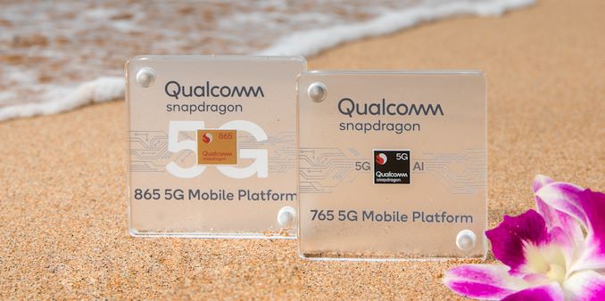
Indeed, this year, Qualcomm isn’t launching just one SoC, but rather two new platforms at the same time. The Snapdragon 865 is self-explanatory in its positioning; as a direct successor to the Snapdragon 855 we expect the new chip to represent the best Qualcomm is able to deliver, and be the silicon that powers most of 2020’s flagship devices. The new top-model this year is accompanied by the new Snapdragon 765 and 765G SoCs. As with other 7-series models since the launch of the new range, the new generation adds of the new features introduced with the new Snapdragon 865, at a lower performance level and a more affordable price for what is becoming an increasingly popular device category.
| Qualcomm Snapdragon Flagship SoCs 2019-2020 | |||
| SoC |
Snapdragon 865 |
Snapdragon 855 | |
| CPU | 1x Cortex A77 @ 2.84GHz 1x512KB pL2 3x Cortex A77 @ 2.42GHz 3x256KB pL2 4x Cortex A55 @ 1.80GHz 4x128KB pL2 4MB sL3 @ ?MHz |
1x Kryo 485 Gold (A76 derivative) @ 2.84GHz 1x512KB pL2 3x Kryo 485 Gold (A76 derivative) @ 2.42GHz 3x256KB pL2 4x Kryo 485 Silver (A55 derivative) @ 1.80GHz 4x128KB pL2 2MB sL3 @ 1612MHz |
|
| GPU | Adreno 650 @ ? MHz +25% perf +50% ALUs +50% pixel/clock +0% texels/clock |
Adreno 640 @ 585 MHz |
|
| DSP / NPU | Hexagon 698 15 TOPS AI (Total CPU+GPU+HVX+Tensor) |
Hexagon 690 7 TOPS AI (Total CPU+GPU+HVX+Tensor) |
|
| Memory Controller |
4x 16-bit CH @ 2133MHz LPDDR4X / 33.4GB/s or @ 2750MHz LPDDR5 / 44.0GB/s 3MB system level cache |
4x 16-bit CH @ 1866MHz LPDDR4X 29.9GB/s 3MB system level cache |
|
| ISP/Camera | Dual 14-bit Spectra 480 ISP 1x 200MP or 64MP with ZSL or 2x 25MP with ZSL 4K video & 64MP burst capture |
Dual 14-bit Spectra 380 ISP 1x 48MP or 2x 22MP |
|
| Encode/ Decode |
8K30 / 4K120 10-bit H.265 Dolby Vision, HDR10+, HDR10, HLG 720p960 infinite recording |
4K60 10-bit H.265 HDR10, HDR10+, HLG 720p480 |
|
| Integrated Modem | none (Paired with external X55 only) (LTE Category 24/22) DL = 2500 Mbps 7x20MHz CA, 1024-QAM UL = 316 Mbps 3x20MHz CA, 256-QAM (5G NR Sub-6 + mmWave) DL = 7000 Mbps UL = 3000 Mbps |
Snapdragon X24 LTE (Category 20) DL = 2000Mbps 7x20MHz CA, 256-QAM, 4x4 UL = 316Mbps 3x20MHz CA, 256-QAM |
|
| Mfc. Process | TSMC 7nm (N7P) |
TSMC 7nm (N7) |
|
We’ll start off with the whole story on the Snapdragon 865, and in particular one surprising aspect what we didn’t expect from the SoC this year; its lack of an integrated modem, and what the story behind the design choice.
No Modem Integration This Year?
The one aspect of the new Snapdragon 865 that overshadows all other new characteristics is the fact that Qualcomm designed it without an integrated modem. Qualcomm already announced this change yesterday during the day 1 of the event, without much context into the matter. It’s been fun seeing the reactions of various media and commenters theorising as to why this would be. It’s also one of the very first aspects that we wanted to have clarified by Qualcomm:
The choice to not integrate the modem this year was a highly practical one, stemming from the complexity of 5G and the platform. There are actually more nuances to this though, and one thing that Qualcomm wants to make clear, is that this isn’t just a matter of the company's technical ability to actually create a chip with an integrated 5G modem; it’s keen to point out the Snapdragon 765, also announced today, which does exactly this.
Instead, the technical difficulty of the 5G modem platform is actually on the platform and device side itself. As this will be the very first wide-range 5G implementation of a lot of OEM vendors who use Qualcomm’s chips, there will be a large number of designs who will be integrating 5G for the first time. The problem is that this requires a quite large development increase for the vendors creating the devices: they need to make sure their RF systems, antenna designs, as well as certifications of the systems are in full order. The nature of the 5G design complexity means that this process in a device’s development cycle this time around is actually quite a lot more complicated and more time-consuming than what we’ve seen from past 4G phones.
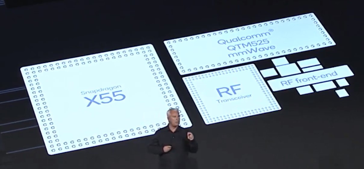
Qualcomm’s solution to the problem, in order to facilitate the vendor’s device development cycle, is to separate the modem from the rest of the application processor, at least for this generation. The X55 modem has had a lead time to market, being available earlier than the Snapdragon 865 SoC by several months. OEM vendors thus would have been able to already start developing their 2020 handset designs on the X55+S855 platform, focusing on getting the RF subsystems right, and then once the S865 becomes available, it would be a rather simple integration of the new AP without having to do much changes to the connectivity components of the new device design.
Qualcomm’s explanation makes a lot of sense in practical terms, and would bring time-to-market advantages. The company explains that in the future, it would re-integrate the modem back into the SoC, and this generation’s choices just made more sense for today’s situation in the market. Qualcomm isn’t the only one to have made such a choice, Samsung’s Exynos 990 SoC makes the same exact design decisions, shipping the main SoC as a simple application processor without any modem, although we don’t have any official backstory on their rationale for the design choice.
The decision of shipping AP+discrete modem does have some disadvantages though. Motherboard PCB complexity does go up this generation, more so than competitors solutions which are able to integrate 5G modems (Such as the HiSilicon Kirin 990 5G, or the MediaTek Dimensity 1000). We also expect some compromises in terms of battery efficiency due to the silicon overhead, however as a counter-argument, Apple’s iPhones always have had separate AP+modem solutions, and the latest generation this year had amongst the strongest battery life performance of any device out there, even with a competing Intel modem.
As for the X55 modem itself: It’s the same piece that Qualcomm announced earlier this year, and this time around promises full global 5G connectivity ability (the X50’s support was more limited). The modem chip is manufactured on the TSMC’s 7nm process node, and the most important fact about the new combination is that the Snapdragon 865 SoC is exclusively tied to the X55 modem. This means that Qualcomm is selling the 865 SoC only as a pair with the X55 modem, and they do not offer support with any past 4G modem. In theory vendors could use another modem, but since they only sell the new platform as a pair anyway, it would make very little sense for anybody to do this.
One question that also came up is on whether vendors, for whatever reason, would still be able to develop 4G phones with the Snapdragon 865+X55 platform. Qualcomm says this would be possible if you essentially just ignore the X55’s 5G capabilities, but they don’t see any reason for any vendor to actually do this. In essence, bar any abnormal decision from some vendors, all Snapdragon 865 devices in 2020 will be full 5G devices.
The Snapdragon 865 Application Processor: TSMC 7nm N7P
With the elephant in the room of the modem configuration being out of the way, we come to the actual Snapdragon 865 application processor.
For me, the biggest surprise of the new chipset was Qualcomm’s revelation that the chip is the fact that it’s manufactured by TSMC on the improved 7nm “N7P” node – this is the same manufacturing process as used by Apple’s A13 chipset. For the longest time were expecting this generation to be manufactured on Samsung’s 7nm EUV process (7LPP), given as the two companies had announcement nearly 2 years ago. It seems that the announcement was actually about the new Snapdragon 765, which does come on the 7LPP process node, and which we'll be covering in more detail later on in the article.
Qualcomm only's comment is that their process node choices were based on various considerations, including volume. Reading between the lines, it’s possible that Qualcomm wasn’t as confident in Samsung’s ability to manufacture the large quantities needed for the new chip. I’ve also heard murmurs from other sources that Samsung’s process simply doesn’t have as good performance and leakage characteristics as TSMC, and in flagship parts, those aspects have to be taken higher consideration than in say a premium- or mid-range SoC. In any case, it’s a big blow to Samsung’s foundry business as having the design win this year was quite critical, as I do not expect them to win the 2021 flagship contract due to TSMC’s 5nm leadership.
As for the choice between TSMC’s N7P and N7+ (+ is the EUV node), it seems HiSilicon is currently the only client for the node for the time being, with the Kirin 990 5G being the only chipset manufactured on the node until later in 2020. It’s most likely that TSMC here simply doesn’t yet have the EUV volume capacity and yields to fulfil Qualcomm’s demand at this point in time, essentially being in a similar situation as Samsung, with the only difference being that TSMC has a viable high-volume DUV-based process ready as an alternative.


91 Comments
View All Comments
Andrei Frumusanu - Wednesday, December 4, 2019 - link
No transistor disclosure from QC. For die sizes, we'll likely have to wait a few months.Raqia - Wednesday, December 4, 2019 - link
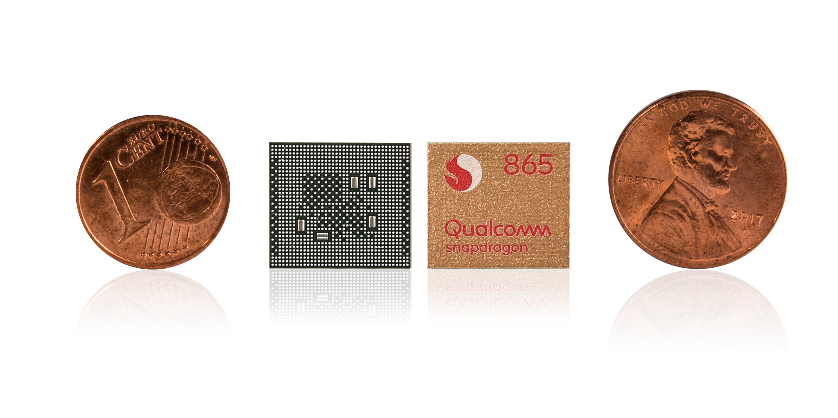
Quick and dirty pixel counting on this pic of a penny (19.05 mm diameter, ~285 mm^2) next to the 865 gives ~200mm^2 for the package:https://cdn.vox-cdn.com/uploads/chorus_asset/file/...
Seems like most of the budget went to the DSP, some to the GPU, and some to the larger caches. Assuming no density changes for N7P, this is about 2.76 times the die area of the 855. According to:
https://www.reddit.com/r/Damnthatsinteresting/comm...
The 855 weighs in at about 6B transistors. Quick and dirty estimate: ~16.55B transistors?
Andrei Frumusanu - Wednesday, December 4, 2019 - link
I'd gather your off in your estimate by about 8-9B transistors.Raqia - Wednesday, December 4, 2019 - link
You're probably right given this shot of the 8cx:https://scdn.slashgear.com/wp-content/uploads/2018...
which weighs in at around 10B transistors at 122mm^2 and has a larger package size. :)
tijag - Wednesday, December 4, 2019 - link
A13 manufactured on this node is 8.5B transistors, doubt strongly the 865 will be much more than that.tijag - Wednesday, December 4, 2019 - link
I see how you got to roughly 200mm^2 for the package but i'm guessing something is off on the scale or the chip is much much smaller than the BGA package its on.skavi - Wednesday, December 4, 2019 - link
I'm going to guess ~85mm^2 with ~7 billion transistors based on the image.Raqia - Wednesday, December 4, 2019 - link
You are probably right. Considering that this bump is from 6 billion - x24 modem transistors, it should be a pretty healthy gain over the 855 in GPU and DSP. Next year's TSMC 5nm process with almost double the transistor density over its 7nm processes should bring far steeper gains even with an integrated x55 modem. I'm fully expecting +75-100% performance gains in GPU and DSP with gobs more cache; their next high end part might warrant a 9xx designation.generalako - Thursday, December 5, 2019 - link
That's assuming to go over to a new architecture as well.I'm more interested about CPU(s). A78, and if ARM will actually get off their asses and give us a successor for the A55, as they seriously need to up their game here, compared to Apple -- both in terms of power efficiency and performance. I'm sure the A78 will continue the 25% IPC improvement trend, which is still very nice, but it's in an A55 successor ARM needs to do something. It's ridiculous how Apple can make a new power-efficient core every single generation, whereas ARM, whose only task is to do this, and who supplies their designs to a huge industry for far more units than iPhones, spend 3 years between them.
Raqia - Thursday, December 5, 2019 - link
There will be more straightforward gains for caches and units besides the CPU with a denser process as those workloads are more embarrassingly parallel even on the same slice/core/module architecture, and the bump from 7nm to 5nm in transistors per mobile SoC will be equal to today's mid-tier desktop GPUs.It's unclear what went into this year's vastly improved Thunder cores in the A13, but at least some of it has to do with Apple's simpler cache hierarchy and ever bigger caches with 8MB of L2 for the 2 large cores, 4MB for the 4 small cores, and a whopping 16MB for the system level L3 cache; the A77 by comparison has 512KB-256k of L2 for the big cores, 128kb of L2 for the little cores, and 4MB of L3 + 3MB of system L4. There's also the fact that they don't need to address server class Neoverse style designs as well with whatever cores they design. Having no need to integrate a modem simplifies Apple's foundry process requirements and lets it devote more die area to its CPU and caches.
As for Android CPUs at 5nm, I could see Android SoCs going to 12 cores on the CPU side or going with more cache per core / CPU complex. I don't expect as much of a single threaded performance change with the Hercules core as it'll get tougher and tougher to wring out more performance from the A76 base design that it will be based on; the successor Matterhorn though... They changed the CPU cluster design greatly with the A75+A55 combo introducing an L3 cache and have seemingly maintained this uncore through A76+A55 and A77+A55; we'll see soon enough if they have a new small design at ARM's techday in May, maybe they'll use the A65AEs next year.