The Intel Optane Memory H10 Review: QLC and Optane In One SSD
by Billy Tallis on April 22, 2019 11:50 AM EST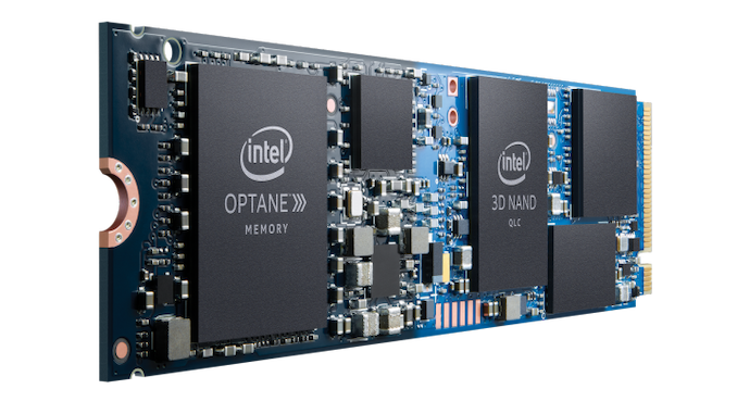
SSD caching has been around for a long time, as a way to reap many of the performance benefits of fast storage without completely abandoning the high capacity and lower prices of slower storage options. In recent years, the fast, small, expensive niche has been ruled by Intel's Optane products using their 3D XPoint non-volatile memory. Intel's third generation of Optane Memory SSD caching products has arrived, bringing the promise of Optane performance to a new product segment. The first Optane Memory products were tiny NVMe SSDs intended to accelerate access to larger slower SATA drives, especially mechanical hard drives. Intel is now supporting using Optane Memory SSDs to cache other NVMe SSDs, with an eye toward the combination of Optane and QLC NAND flash. They've put both types of SSD onto a single M.2 module to create the new Optane Memory H10.
The Intel Optane Memory H10 allows Intel for the first time to put their Optane Memory caching solution into ultrabooks that only have room for one SSD, and have left SATA behind entirely. Squeezing two drives onto a single-sided 80mm long M.2 module is made possible in part by the high density of Intel's four bit per cell 3D QLC NAND flash memory. Intel's 660p QLC SSD has plenty of unused space on the 1TB and 512GB versions, and an Optane cache has great potential to offset the performance and endurance shortcomings of QLC NAND. Putting the two onto one module has some tradeoffs, but for the most part the design of the H10 is very straightforward.
The Optane Memory H10 does not introduce any new ASICs or any hardware to make the Optane and QLC portions of the drive appear as a single device. The caching is managed entirely in software, and the host system accesses the Optane and QLC sides of the H10 independently. Each half of the drive has two PCIe lanes dedicated to it. Earlier Optane Memory SSDs have all been PCIe x2 devices so they aren't losing anything, but the Intel 660p uses a 4-lane Silicon Motion NVMe controller, which is now restricted to just two lanes. In practice, the 660p almost never needed more bandwidth than an x2 link can provide, so this isn't a significant bottleneck.
| Intel Optane Memory H10 Specifications | |||||
| Advertised Capacity | 256 GB | 512 GB | 1TB | ||
| Form Factor | single-sided M.2 2280 | ||||
| NAND Controller | Silicon Motion SM2263 | ||||
| NAND Flash | Intel 64L 3D QLC | ||||
| Optane Controller | Intel SLL3D | ||||
| Optane Media | Intel 128Gb 3D XPoint | ||||
| QLC NAND Capacity | 256 GB | 512 GB | 1024 GB | ||
| Optane Capacity | 16 GB | 32 GB | 32 GB | ||
| Sequential Read | 1450 MB/s | 2300 MB/s | 2400 MB/s | ||
| Sequential Write | 650 MB/s | 1300 MB/s | 1800 MB/s | ||
| Random Read IOPS | 230k | 320k | 330k | ||
| Random Write IOPS | 150k | 250k | 250k | ||
| L1.2 Idle Power | < 15 mW | ||||
| Warranty | 5 years | ||||
| Write Endurance | 75 TB 0.16 DWPD |
150 TB 0.16 DWPD |
300 TB 0.16 DWPD |
||
With a slow QLC SSD and a fast Optane SSD on one device, Intel had to make judgement calls in determining the rated performance specifications. The larger two capacities of H10 are rated for sequential read speeds in excess of 2GB/s, reflecting how Intel's Optane Memory caching software can fetch data from both QLC and Optane portions of the H10 simultaneously. Writes can also be striped, but the maximum rating doesn't exceed any obvious limit for single-device performance. The random IO specs for the H10 fall between the performance of the existing Optane Memory and 660p SSDs, but are much closer to Optane performance. Intel's not trying to advertise a perfect cache hit rate, but they expect it to be pretty good for ordinary real-world usage.
The Optane cache should help reduce the write burden that the QLC portion of the H10 has to bear, but Intel still rates the whole device for the same 0.16 drive writes per day that their 660p QLC SSDs are rated for.
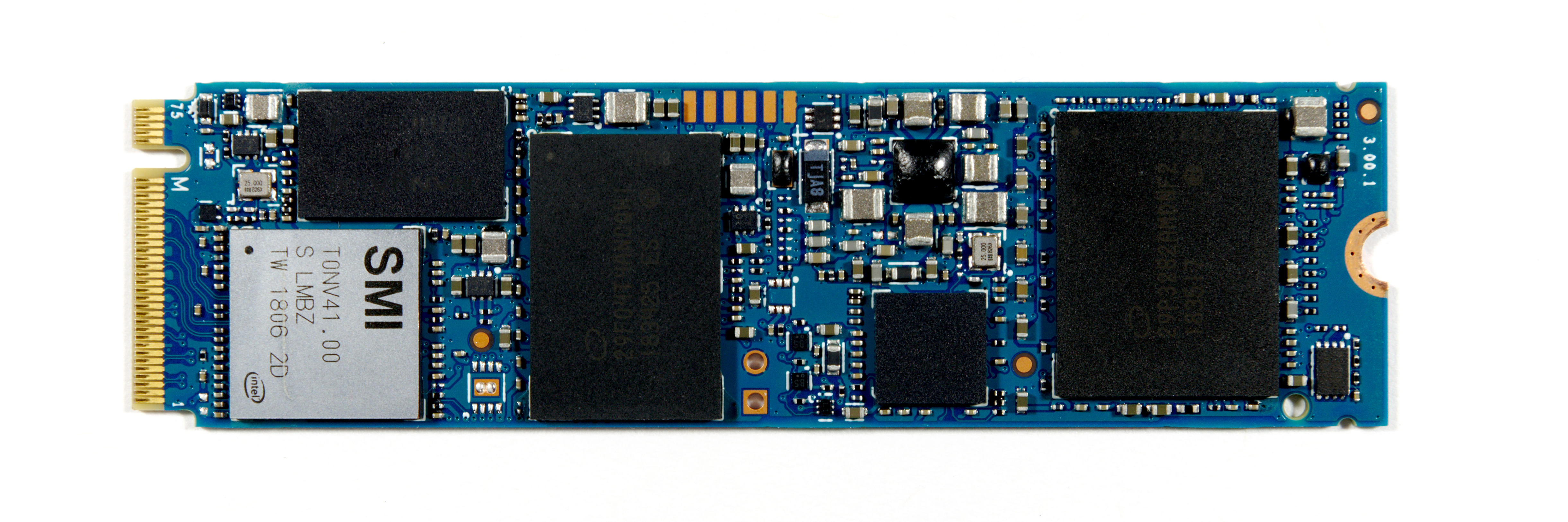


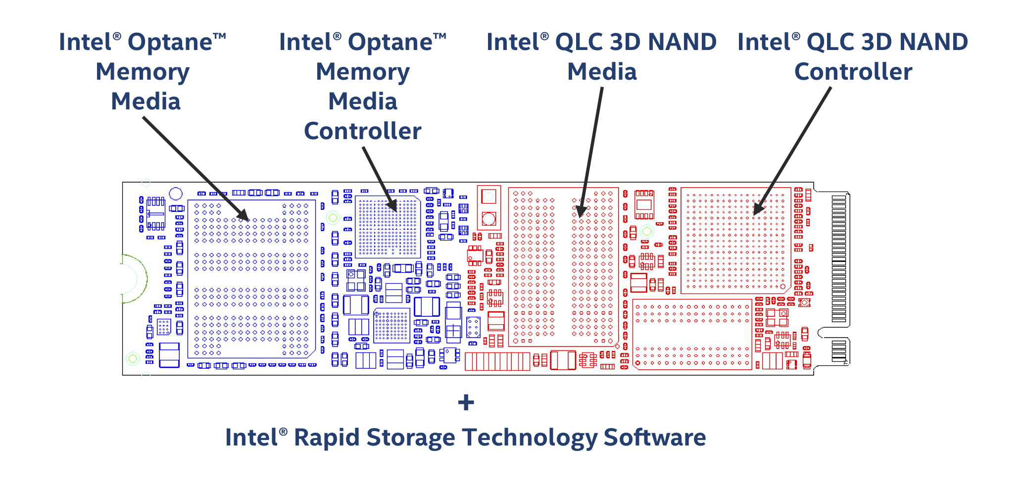
Intel's marketing photos of the Optane Memory H10 show it with a two-tone PCB to emphasize the dual nature of the drive, but in reality it's a solid color. The PCB layout is unique with two controllers and three kinds of memory, but it is also obviously reminiscent of the two discrete products it is based on. The QLC NAND half of the drive is closer to the M.2 connector and features the SM2263 controller and one package each of DRAM and NAND. The familiar Silicon Motion test/debug connections are placed at the boundary between the NAND half and the Optane half. That Optane half contains Intel's small Optane controller, a single package of 3D XPoint memory, and most of the power management components. Both the Intel SSD 660p and the earlier Optane Memory SSDs had very sparse PCBs; the Optane Memory H10 is crowded and may have the highest part count of any M.2 SSD on the market.
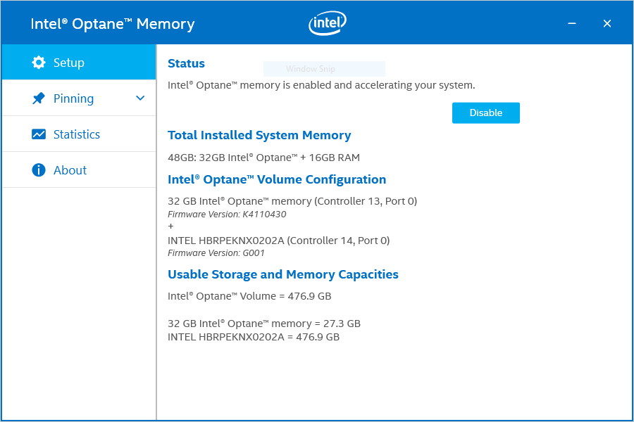
On the surface, little has changed with the Optane Memory software; there's just more flexibility now in which devices can be selected to be cached. (Intel has also opened extended Optane Memory support to Pentium and Celeron branded processors on platforms that were already supported with Core processors.) When the boot volume is cached, Intel's software allows the user to specify files and applications that should be pinned to the cache and be immune from eviction. Other than this, there's no room for tweaking of the cache behavior.
Some OEMs that sell systems equipped with Optane Memory have been advertising memory capacities as the sum of DRAM and Optane capacities, which might be reasonable if we were talking about Optane DC Persistent Memory modules that connect to the CPU's memory controller, but is very misleading when the Optane product in question is an SSD. Intel says to blame the OEMs for this misleading branding, but Intel's own Optane Memory software does the same thing.
Initially, the Optane Memory H10 will be an OEM-only part, available to consumers only pre-installed in new systems—primarily notebooks. Intel is considering bringing the H10 to retail both as a standalone product and as part of a NUC kit, but they have not committed to plans for either. Their motherboard partners have been laying the groundwork for H10 support for almost a year, and many desktop 300-series motherboards already support the H10 with the latest publicly available firmware.
Platform Compatibility
Putting two PCIe devices on one M.2 card is novel to say the least. Intel has put two SSD controllers on one PCB before with high-end enterprise drives like the P3608 and P4608, but those drives use PCIe switch chips to split an x8 host connection into x4 for each of the two NVMe controllers on board. That approach leads to a 40W TDP for the entire card, which is not at all useful when trying to work within the constraints of a M.2 card.
There are also several PCIe add-in cards that allow four M.2 PCIe SSDs to be connected through one PCIe x16 slot. A few of these cards also include PCIe switches, but most rely on the host system supporting PCIe port bifurcation to split a single x16 port into four independent x4 ports. Mainstream consumer CPUs usually don't support this, and are generally limited to x8+x4+x4 or just x8+x8 bifurcation, and only when the lanes are being re-routed to different slots to support multi-GPU use cases. Recent server and workstation CPUs are more likely to support bifurcation down to x4 ports, but motherboard support for enabling this functionality isn't universal.
Even on CPUs where an x16 slot can be split into four x4 ports, further bifurcation down to x2 ports is seldom or never possible. The chips that do support operating a lot of PCIe lanes as narrow x2 or x1 ports are the southbridge/PCH chips on most motherboards. These tend to not support ports any wider than x4, because that's the normal width of the connection upstream to the CPU.
Based on the above, we put theory to the test and tried the Optane Memory H10 with almost every PCIe 3.0 port we had on hand, using whatever adapters were necessary. Our results are summarized below:
| Intel Optane Memory H10 Platform Compatibility |
||||||
| Platform | PCIe Source |
NAND Usable |
Optane Usable |
Optane Memory Caching |
||
| Whiskey Lake | PCH | Yes | Yes | Yes | ||
| Coffee Lake | CPU | Yes | No | No | ||
| PCH | Yes | Yes | No* | |||
| Kaby Lake | CPU | Yes | No | No | ||
| PCH | Yes | No | No | |||
| Skylake | CPU | Yes | No | No | ||
| PCH | Yes | No | No | |||
| Skylake-SP (Purley) |
CPU | Yes | No | No | ||
| PCH | Yes | No | No | |||
| Threadripper | CPU | No | Yes | No | ||
| Avago PLX Switch | Yes | No | No | |||
| Microsemi PFX Switch | No | Yes | No | |||
The Whiskey Lake notebook Intel provided for this review is of course fully compatible with the Optane Memory H10, and will be available for purchase in this configuration soon. Compatibility with older platforms and non-Intel platforms is mostly as expected, with only the NAND side of the H10 accessible—those motherboards don't expect to find two PCIe devices sharing a physical M.2 x4 slot, and aren't configured to detect and initialize both devices. There are a few notable exceptions:
First, the H370 motherboard in our Coffee Lake system is supposed to fully support the H10, but GIGABYTE botched the firmware update that claims to have added H10 support: both the NAND and Optane portions of the H10 are accessible when using a M.2 slot that connects to the PCH, but it isn't possible to enable caching. There are plenty of 300-series motherboards that have successfully added H10 support, and I'm sure GIGABYTE will release a fixed firmware update for this particular board soon. Putting the H10 into a PCIe x16 slot that connects directly to the CPU does not provide access to the Optane side, reflecting the CPU's lack of support for PCIe port bifurcation down to x2+x2.
The only modern AMD system we had on hand was a Threadripper/X399 motherboard. All of the PCIe and M.2 slots we tried led to the Optane side of the H10 being visible instead of the NAND side.
We also connected the H10 through two different brands of PCIe 3.0 switch. Avago's PLX PEX8747 switch only provided access to the NAND side, which is to be expected since it only supports PCIe port bifurcation down to x4 ports. The Microsemi PFX PM8533 switch does claim to support bifurcation down to x2 and we were hoping it would enable access to both sides of the H10, but instead we only got access to the Optane half. The Microsemi switch and Threadripper motherboard may both be just a firmware update away from working with both halves of the H10, and earlier Intel PCH generations might also have that potential, but Intel won't be providing any such updates. Even if these platforms were able to access both halves of the H10, they would not be supported by Intel's Optane Memory caching drivers, but third-party caching software exists.


60 Comments
View All Comments
Flunk - Monday, April 22, 2019 - link
This sounded interesting until I read software solution and split bandwidth. Intel seems to be really intent upon forcing Optane into products regardless if they make sense or not.Maybe it would have made sense with SSDs at the price points they were this time last year, but now it just seems like pointless exercise.
PeachNCream - Monday, April 22, 2019 - link
Who knew Optane would end up acting as a bandage fix for QLC's garbage endurance? I suppose its better than nothing, but 0.16 DWPD is terrible. The 512GB model would barely make it to 24 months in a laptop without making significant configuration changes (caching the browser to RAM, disabling the swap file entirely, etc.)IntelUser2000 - Monday, April 22, 2019 - link
The H10 is a mediocre product, but endurance claims are overblown.Even if the rated lifespan is a total of 35TB, you'd be perfectly fine. The 512GB H10 is rated for 150TB.
The amount of users that would even reach 20TB in 5 years are in the minority. When I was actively using the system, my X25-M registered less than 5TB in 2 years.
PeachNCream - Monday, April 22, 2019 - link
Your usage is extremely light. Endurance is a real-world problem. I've already dealt with it a couple of times with MLC SSDs.IntelUser2000 - Monday, April 22, 2019 - link
SSDs are over 50% of the storage sold in notebooks. It's firmly reaching mainstream there.I would say instead I think most of *your* customers are too demanding. Vast majority of the folks would use less than me.
The market agrees too, which is why we went from MLC to TLC, and now we have QLCs coming.
Perhaps you are confusing write-endurance with physical stress endurance, or even natural MTBF related endurance.
PeachNCream - Monday, April 22, 2019 - link
I haven't touched on any usage but my own so far. The drives' own software identified the problems so if there is confusion about failures, that's in the domain of the OEM. (Note, those drives don't fail gracefully either so that data can be recovered. It's a pretty ugly end to reach.) As for the move from MLC to TLC and now QLC -- thats driven by cost sensitivity for given capacities and ignores endurance to a great extent.IntelUser2000 - Monday, April 22, 2019 - link
I get the paranoia. The world does that to you. You unconsciously become paranoid in everything.However, for most folks endurance is not a problem. The circuit in the SSD will likely fail of natural causes before write endurance is reached. Everything dies. But people are just excessively worried about NAND SSD write endurance because its a fixed metric.
It's like knowing the date of your death.
PeachNCream - Friday, May 3, 2019 - link
That's not really a paranoia thing. You're attempt to bait someone into an argument where you can then toss out insults is silly.SaberKOG91 - Monday, April 22, 2019 - link
That's a naive argument. Most SSDs of 250GB or larger are rated for at least 100TBW on a 3 year warranty. 75TBW on a 5 year warranty is an insult.I think you underestimate how much demand the average user makes of their system. Especially when you have things like anti-virus and web browsers making lots of little writes in the background, all the time.
The market is going from TLC to QLC because of density, not reliability. We had all the same reliability issues going from MLC to TLC and from SLC to MLC. It took years for each transition for manufacturers to reach the same durability level as the previous technology, all while seeing the previous generation continuing to improve even further. Moving to denser tech means smaller dies for the same capacity or higher capacity for unit area which is good for everyone. But these drives don't even look to have 0.20DWPD or 5 year warranty of other QLC Flash products.
I am a light user who doesn't have a lot of photos or video and this laptop has already seen 1.3TBW in only 3 months. My work desktop has over 20TBW from the last 5 years. My home desktop where I compile software has over 12TBW in the first year. My gaming PC has 27TBW on a 5 year old drive. So while I might agree that 75TBW seems like a lot, If I were to simplify my life down to one machine, I'd easily hit 20TBW a year or 8TBW a year even without the compile machine.
That all said, you're still ignoring that many Micron and Samsung drives have been shown to go way beyond their rated lifespan whereas Optane has such horrible lifespan at these densities that reviewers destroyed the drives just benchmarking them. Since the Optane is acting as a persistent cache, what happens to these drives when the Optane dies? At the very least performance will tank. At the worst the drive is hosed.
IntelUser2000 - Monday, April 22, 2019 - link
Something is very wrong with your drive or you are not really a "light user".1300GB in 3 months equals to 14GB write per day. That means if you use your computer 7 hours a day you'd be using 2GB/s hour. The computer I had the SSD on I used it for 8-12 hours every day for the two years and it was a gaming PC and a primary one at that.
Perhaps the X25-M drive I had is particularly good at this aspect, but the differences seem too much.
Anyways, moving to denser cells just mean consumer level workloads do not need the write endurance MLC needs and lower prices are preferred.
"Optane has such horrible lifespan at these densities that reviewers destroyed the drives just benchmarking them."
Maybe you are referring to the few faulty units in the beginning? Any devices can fail in the first 30 days. That's completely unrelated to *write endurance*. The first gen modules are rated for 190TBW. If they played around for a year(which is unrealistic since its for a benchmark), they would have been using 500GB/s day. Maybe you want to verify your claims yourself.