Western Digital’s RISC-V "SweRV" Core Design Released For Free
by Anton Shilov on February 15, 2019 11:30 AM EST- Posted in
- Storage
- CPUs
- SSDs
- Western Digital
- RISC-V

Western Digital has published a register-transfer level (RTL) design abstraction of its in-house designed SweRV RISC-V core. The SweRV core is one of several RISC-V projects the company as undertaken as part of their effort to spearhead the ISA, its ecosystem, and foster their own transition away from licensed, royalty-charging CPU cores. In accordance with the more open design goals of RISC-V, the publication of the high-level representation of SweTV means that third parties can use it in their own chip designs, which will popularize not only the particular core design, but also the RISC-V architecture in general.
The RTL design abstraction of Western Digital’s RISC-V SweRV core is now available at GitHub. The design is licensed under the Apache 2.0 license, which is a very permissive (and non-copyleft) license that allows the core to be used free of charge, with or without modifications, and without requiring any modifications to be released in-kind. In fact the requirements of the license are quite slim; besides requiring appropriate attribution, the only other notable restriction is that third party developers cannot use Western Digital’s brands to mark their work.
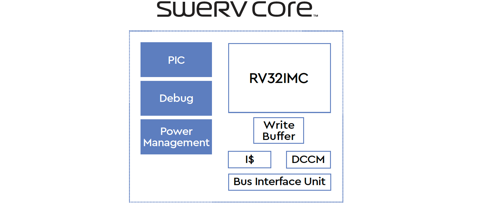
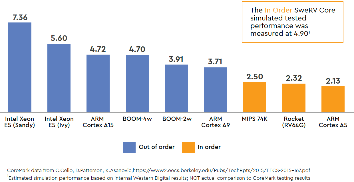
Western Digital’s RISC-V SweRV core is a 32-bit in-order core featuring a 2-way superscalar design and a nine-stage pipeline. When implemented using a 28 nm process technology, the core runs at up to 1.8 GHz. Based on Western Digital’s simulations, the SweRV core delivers 4.9 CoreMark/MHz, which is a bit higher when compared to ARM’s Cortex-A15. The developer of the core plans to use its RISC-V cores for its own embedded designs, such as flash controllers and SSDs, but it is unclear when these chips are set to be available.
Being one of the major supporters of RISC-V, Western Digital believes that by letting third-parties to use the core it will help to drive adoption of the RISC-V architecture by hardware and software designers. The latter will ensure that Western Digital’s own future designs will get a better support by software developers.
Related Reading:
- Western Digital Reveals SweRV RISC-V Core, Cache Coherency over Ethernet Initiative
- Western Digital to Use RISC-V for Controllers, Processors, Purpose-Built Platforms
- SiFive Unveils Freedom Platforms for RISC-V-Based Semi-Custom Chips
Source: Western Digital/Github


14 Comments
View All Comments
peevee - Friday, February 15, 2019 - link
Bad testing. What do you expect from Berkley these days?kfishy - Friday, February 15, 2019 - link
The Sandy Bridge number is the CoreMark certified result, presumably from Intel themselves, whereas Ivy Bridge was benchmarked by the researchers themselves. That probably explains the difference.kfishy - Friday, February 15, 2019 - link
This is the paper WD got their numbers from. https://www2.eecs.berkeley.edu/Pubs/TechRpts/2015/...Wilco1 - Friday, February 15, 2019 - link
There is a long history from the MIPS days to make bogus benchmark comparisons. For example MIPS used to add a pass in GCC which improves Coremark by ~30%. They then quote numbers for MIPS with the pass enabled and for their competitors with the pass disabled eventhough the pass worked equally well for them. That pass is on by default in GCC nowadays, however the trick now is to use an old GCC version for the competition...