Intel’s Keynote at CES 2019: 10nm, Ice Lake, Lakefield, Snow Ridge, Cascade Lake
by Ian Cutress on January 7, 2019 7:45 PM EST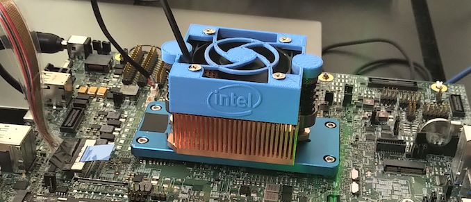
This year it seems that Intel is finally ready to talk about 10nm. After next-to-nothing on the subject at CES 2018, Intel is now talking about three new processor families: Ice Lake, Lakefield, and Snow Ridge. Despite the naming, it looks like Intel might be coming in out of the cold – to finally let it go – and roadmaps on upcoming products are being discussed.
It should be pointed out that Intel’s presentation did not mention anything about the company’s search for a new CEO, or any updates about Intel’s increased demand for its high-end Xeon processors. These are matters that the company will no doubt want to save for their earnings release later this month.
Stage 1: Consumer
Intel Client Group SVP Gregory Bryant took to the stage for Intel to announce two major hardware platforms and a new initiative in mobile computing. These were Ice Lake, Lakefield, and Project Athena.
Ice Lake: First Volume 10nm
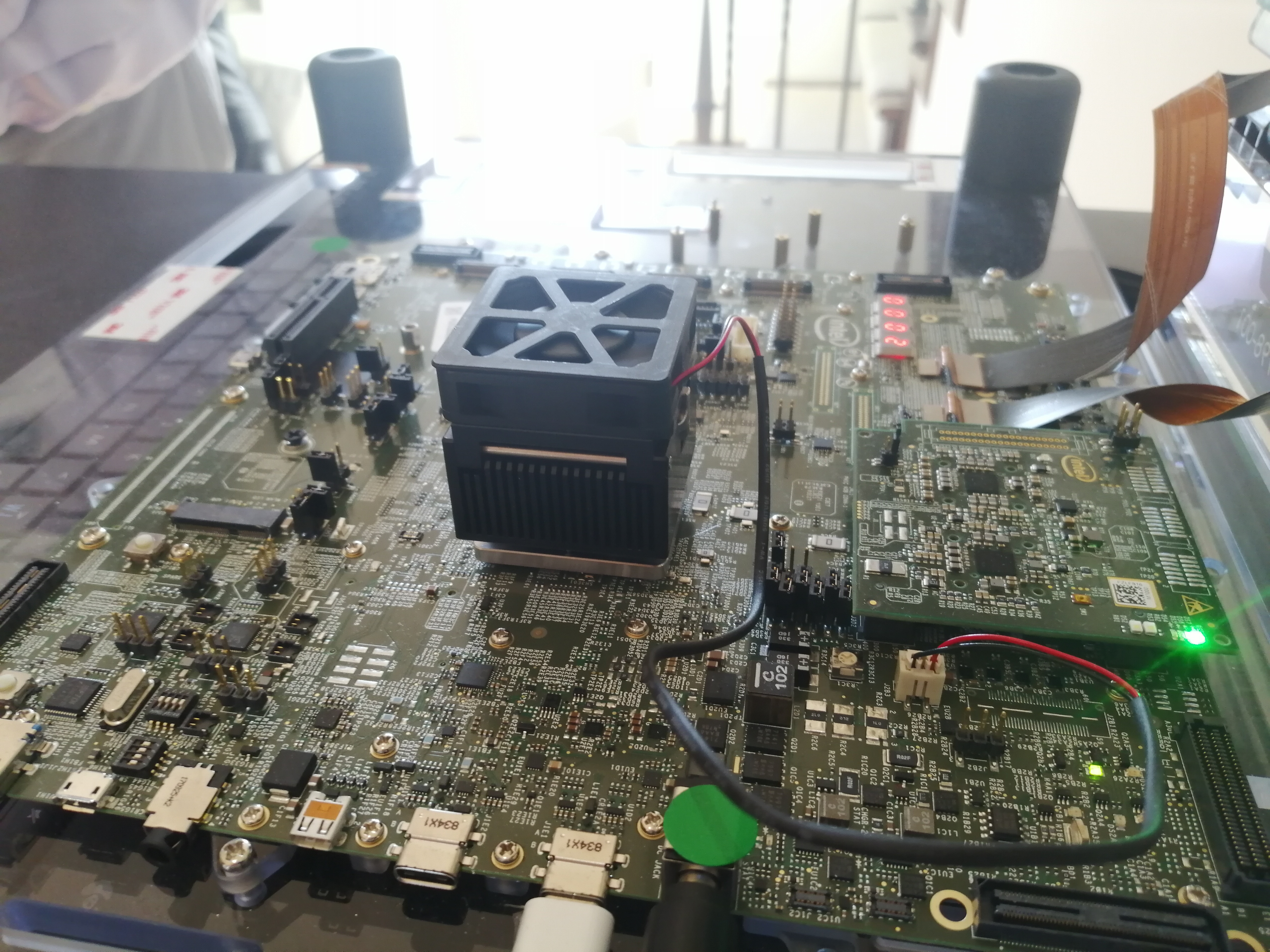
One of the topics discussed at Intel’s Architecture Day, but under embargo until this week, is Intel’s vision for its first generation of 10nm-class consumer processors. We had already been given some details about Sunny Cove, the new Core design, as well as the updated Gen11 graphics architecture, but it will be Ice Lake that puts them both together.
Ice Lake, or more specifically Ice Lake-U it would appear, will be Intel’s first volume client processor on 10nm. Mobile processors are usually small, so it makes sense for Intel to use one for their first volume part in order to balance yields and costs – we’ve seen it before with 14nm, where Broadwell-U entered the market first. The base design from Intel looks to have four cores, eight threads, and 64 GPU execution units for graphics. Intel stated that they are driving the die area even more towards graphics under Gen11 in order to get more performance. This will be, according to Intel, its first standard (GT2-class) processor with 1 TFLOP of integrated graphics performance.
| Intel Ice Lake '4+2' For Notebooks | |
| Manufacturing Process | Intel 10nm |
| Cores / Threads | 4 / 8 |
| CPU Microarchitecture | Sunny Cove |
| Graphics Microarchitecture | Gen11 |
| Graphics Execution Units | GT2, 64 |
| TDP | 15W |
| Memory | LPDDR4X - yes LPDDR4X-3200 ? |
| Memory Bandwidth | 50-60 GB/s |
| Connectivity | TB3 over Type-C Wi-Fi 6 (802.11ax) with CRF |
| Image Processing Unit | 4th Gen |
Hardware wise, Intel explained that these processors would be using LPDDR4X. In a different segment of the presentation it was mentioned that the increase in integrated graphics (from a 24 EU configuration to a 64 EU configuration) required increasing memory bandwidth up to at least 50 GB/s. Intel did not disclose the specific memory frequencies supported, but with these bits of information I’d put LPDDR4X-3200 as the lower bound, as it offers 51.2 GB/s of bandwidth in dual channel mode. This is surprising, given that Intel is usually conservative with supported memory speed declarations – they still make a DDR4-2933 processor in their lineup – so jumping to 3200 would indeed be an unexpected shift for the company.
On the connectivity side, the chipsets for Ice Lake will enable Wi-Fi 6 (802.11ax) over the CNVi interface when an appropriate Intel CRF module is installed. Native Thunderbolt 3 is also expected, which of course operates over USB Type-C connections. Intel reworked the interface for camera support as well, adjusting the interface such that a MIPI-to-USB chip is no longer needed in a laptop bezel for webcam support.
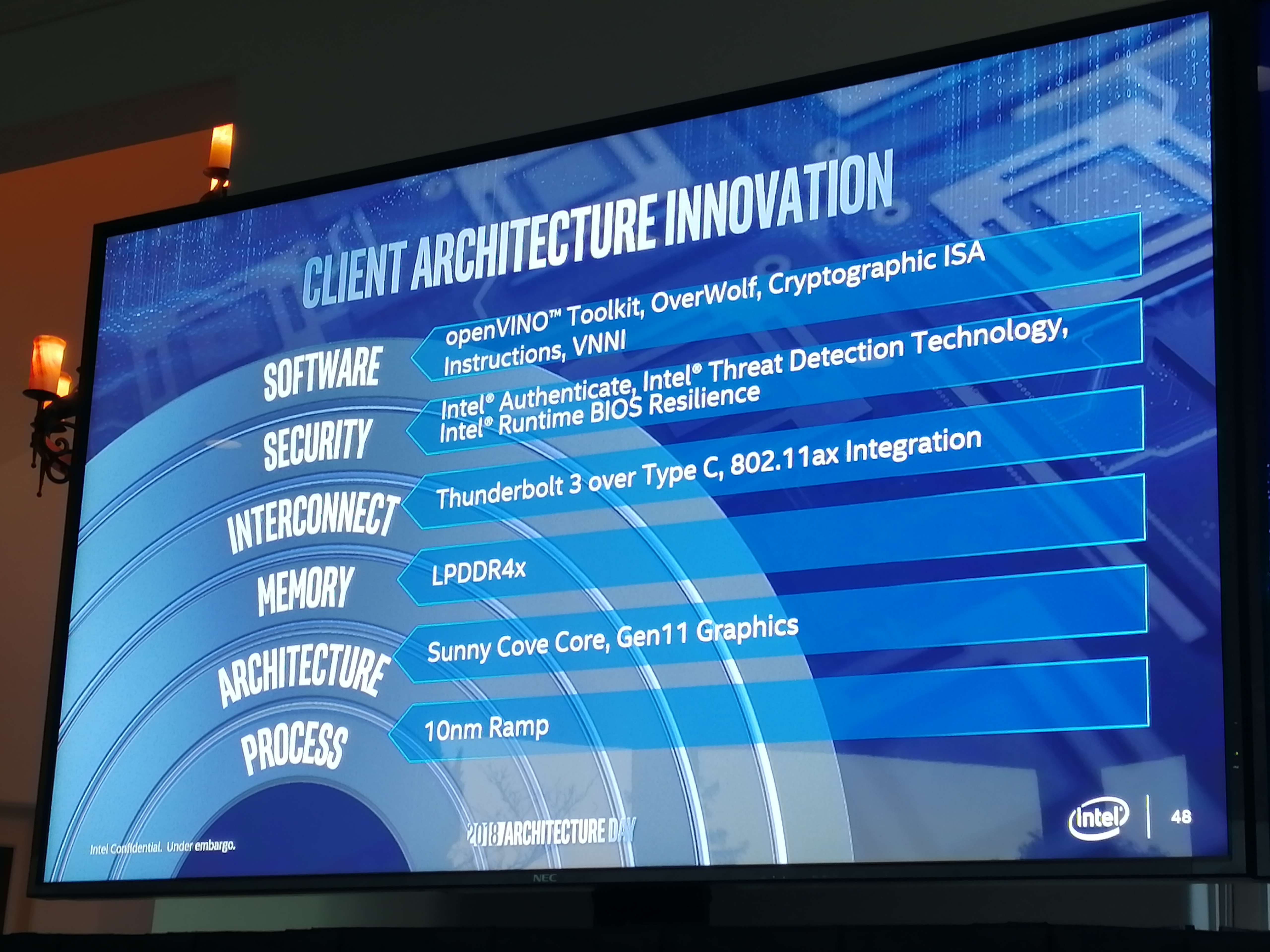
Intel also mentioned software support, such as the new VNNI instructions, openVINO toolkit support, Cryptographic ISA instructions, and support for Overworld. These processors will have at least a similar security level as Cascade Lake, with hardware-enabled Spectre v2 mitigations.
Intel's Image Processing Unit, or IPU, is also upgraded to a fourth generation model. This part of the chip, according to Intel, now has a concurrent imaging pipeline for machine learning, and can support a single IR/RGB camera for login (e.g. Windows Hello). The IPU's power plane has also been tweaked, giving it more performance/power states so the system can save power as needed.
Ice Lake Designs: More Battery Life
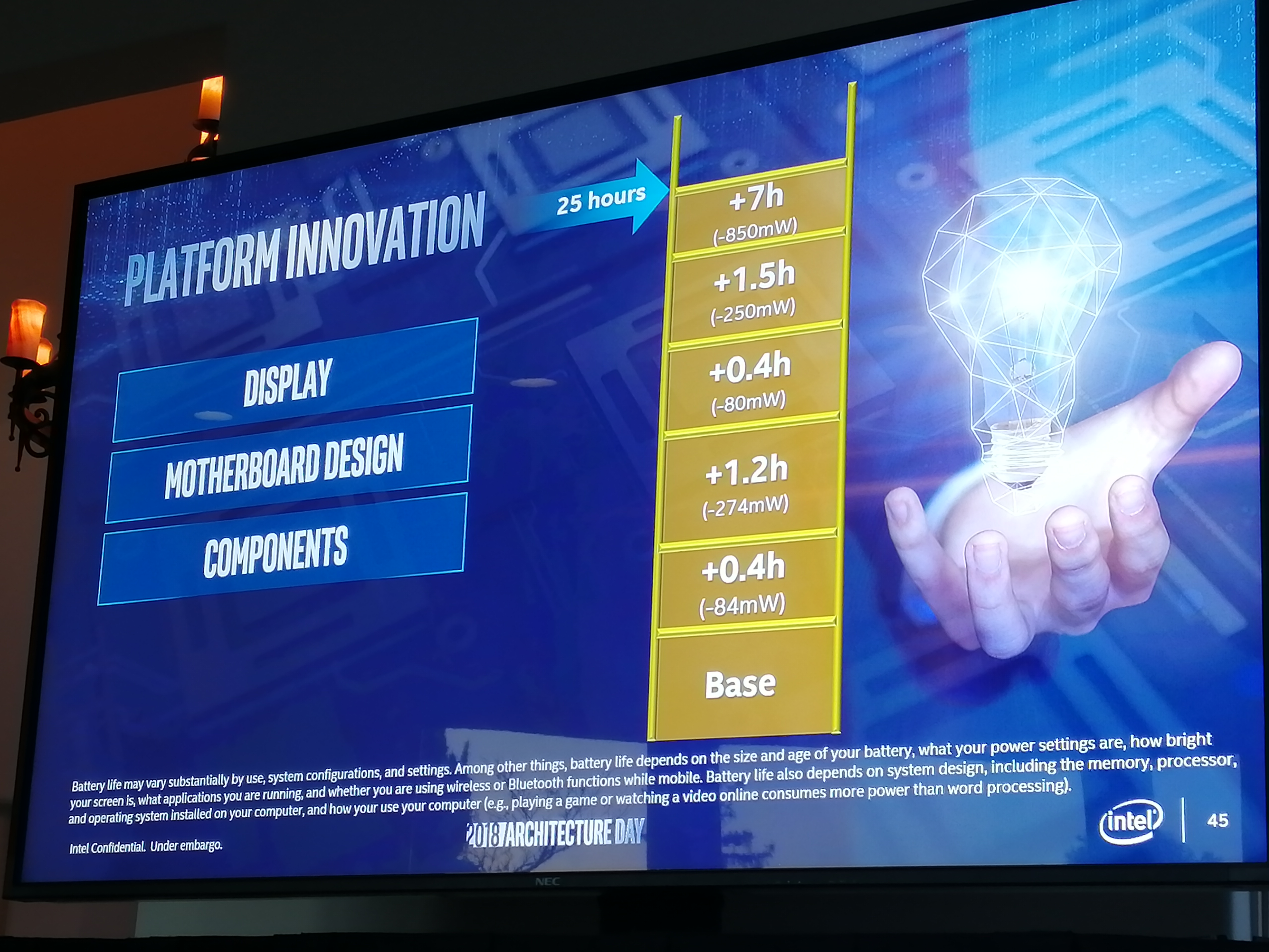
Beyond the 10nm process node change, Intel also announced two additional ways in which it was improving battery life for Ice Lake-U systems. Firstly, the company described its efforts on platform innovation, saying they did a top-to-bottom analysis of what in the system is drawing power and finding ways to reduce it while still keeping performance. As a result, combined with the new ‘1W’ display technologies the company introduced at Computex in June, we’ve been told that optimized Intel devices should now be able to achieve 25+ hours of battery life.
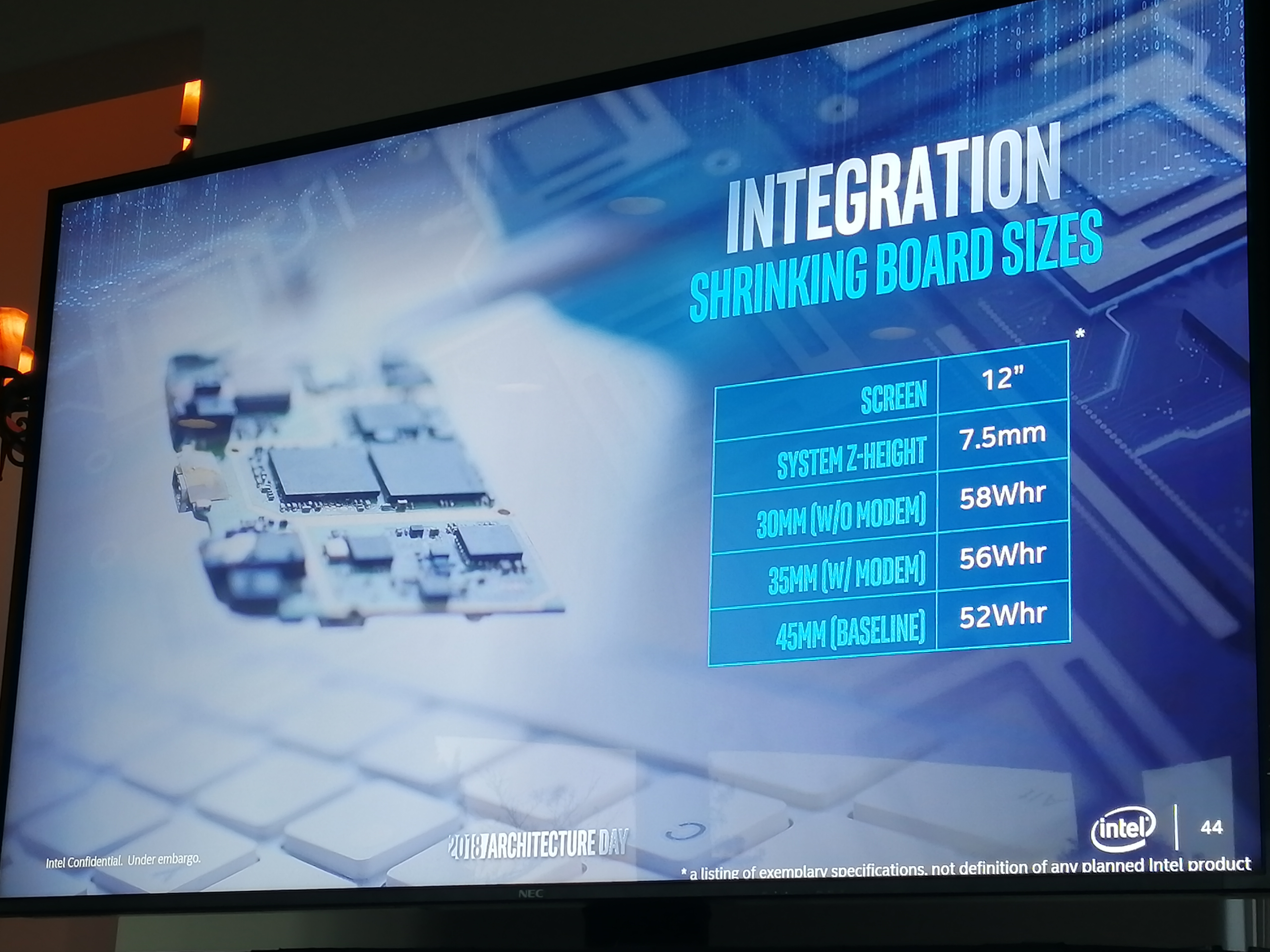
Following a similar line of reasoning, Intel also reworked the board design specifications for thin and light devices. For a typical 12-inch laptop, Intel has freed up room for about 10% more battery capacity – going from 52 Wh to 58 Wh – thanks to reducing the total z-height and x/y dimensions of the motherboard. Interestingly, they've accomplished this without reducing the component count, bringing down the board size while retaining a given number of components.
Lakefield: Foveros Technology Coming Soon
At Intel’s Architecture Day in December, we saw a new class of chip from the company: a hybrid x86 CPU. It was a big announcement for two reasons: the first was that it featured both Core architecture and Atom architecture CPU cores, something that Intel had never done before. Ever since Arm's success with the similar concept of big.Little designs, we have been expecting Intel to come out with some products following this idea, but it was big news that this was finally the time. The second reason for it being a big announcement is that it used ‘Foveros’, Intel’s 3D active interposer technology that puts the cores and graphics on a chip on an interposer. However in a wrinkle from other interposer-based solutions, Foveros but puts the IO in the interposer (rather than using the interposer as a 'dumb' piece of silicon to route signals) all with through-silicon vias to make it work. A chip like this is much smaller in the x/y dimensions, as well as showcasing some very nice packaging technology.
Intel is giving that chip an official family name: Lakefield. The goal of designing Lakefield came from an OEM request to develop a chip that had 2 mW idle power draw, something much lower than current designs. Thus Lakefield was created. It uses a single Sunny Cove core, four Tremont Atom cores, and Gen11 graphics, all built on 10nm.

There have been questions about where exactly this chip will end up, or who even asked for it in the first place. Intel has stated that while a single customer put in the request, Lakefield will be available to all OEM partners if they want to design products around it. A lot of discussion has been held that this was an Apple request, and given Apple’s device portfolio, its volume of sales, and its desire to drive down power with optimized unique designs, the argument for Apple holds some water. But it doesn't sit right with me. This is more a low-powered chip, perhaps even lower power than the A12X in the iPads, so I don’t think Apple would want that chip in one of its MacBooks. (When we asked at architecture day, they said the chip could easily compete at the 7W TDP range, but I imagine it could go lower if needed.) Personally I’m of the opinion that it’s for the dual-screen Lenovo Yogabook. That device is super thin, super light, powers an LCD display and an eInk-like display, and doesn’t need that much power to do what it needs to do. But because it’s so thin there's limited room for battery cells, meaning that power consumption and the resulting battery life are all important, which is where Lakefield is likely to excel.
Intel announced that Lakefield was expected to be in production for products in 2019, which aligns with Intel’s commitment to having 10nm devices on shelves for the holiday season in 2019 (which would mean Christmas 2019).
Project Athena: Building Devices Ready for AI and 5G
As the single biggest force behind the PC ecosystem – and yet not a company that's selling hardware directly to consumers in most cases – Intel enjoys creating programs that try and push the market in certain directions. Depending on who you talk to, the Ultrabook program was either a big failure or a big success, but in the end it did give OEMs a chance to play with thin and light designs for a few years before the hardware gave users a good user experience and battery life. Project Athena is something slightly different, in that it will be a program for Intel and OEMs to work together to enable new experiences with technology coming in the next decade.
Terms like ‘5G’ and ‘Artificial Intelligence’ are only going to become more ubiquitous through 2020 and beyond, so Intel is jumping on it today. Current connectivity experiences for notebooks and laptops vary significantly, and AI implementations are either basic or removed from the local machine entirely and processed in cloud servers. With Project Athena, Intel is going to discuss with OEMs, with partners, customers, software developers, etc. what they need in order to enable these new terms to provide a good user experience. It isn’t just limited to 5G and AI, but we might see more requests for better AI toolkits, or power optimized designs for mobile connectivity, or more compute-related acceleration. It also extends to OEMs in their device design – if an OEM needs several cameras, or new biometrics, or supports more gestures, or new microphone array capabilities etc.
As this is a new program based in aspirational discussion followed by execution, it is unclear what the end goal will look like, only that the aim is around improvements to user experiences.
New 9th Gen Core CPUs
Intel also announced, briefly, that they will be releasing six new desktop 9th Gen Core processors, from Core i3 to Core i9. It did not disclose which parts or what the specifciations are, however we assume they will be available soon. We found the parts listed on Intel's ARK database just after the keynote and you can read our writeup here.
Also in the 9th Gen space, Intel said that the mobile 9th Gen Core processors will be available in Q2.


60 Comments
View All Comments
PeachNCream - Tuesday, January 8, 2019 - link
In the original Legend of Zelda, the Overworld was the exterior areas above any dungeon in which a piece of the Triforce was stored. I presume this means that Intel is ensuring software support for such top-level areas, but refuses to actually do anything to reassemble the Triforce.KPOM - Tuesday, January 8, 2019 - link
Any word on when the Ice Lake-Y chips will be available, and whether they will support LP-DDR4X and Thunderbolt 3?sbrown23 - Tuesday, January 8, 2019 - link
"A lot of discussion has been held that this was an Apple request, and given Apple’s device portfolio, its volume of sales, and its desire to drive down power with optimized unique designs, the argument for Apple holds some water. But it doesn't sit right with me. This is more a low-powered chip, perhaps even lower power than the A12X in the iPads, so I don’t think Apple would want that chip in one of its MacBooks."I'm going with Microsoft. Seems perfect for a next-gen Surface Go.Current one is clocked too low, weak GPU, and dual-core with no HT. The Foveros 10nm SoC would give them an improvement so many ways: lower idle power draw, probably a better GPU, increased core count with the Tremont cores, and likely a much higher clock on the Sunny Cove core for single core burst duties than they have on the current 1.6GHz Pentium Gold.
Given that Qualcomm is a long way from matching Apple's A12 performance, Lakefield in Surface Go seems like a perfect fit.
ilkhan - Tuesday, January 8, 2019 - link
*yawn*.Wake me up when Intel actually releases a meaningful upgrade instead of yet another 2-3% of worthless.
iwod - Tuesday, January 8, 2019 - link
We will have to wait for Lakefield Pricing. If it is sub $50, may be we could see a $899 MacBook.peevee - Tuesday, January 8, 2019 - link
"This is surprising, given that Intel is usually conservative with supported memory speed declarations – they still make a DDR4-2933 processor in their lineup – so jumping to 3200 would indeed be an unexpected shift for the company."Frequency increase of 9% is not jump, it is a tiny half-step. But LPDDR4x instead of hopelessly outdated and power-hungry DDR4 is a very different matter, both in mobile and (would be) server space.
Hixbot - Tuesday, January 8, 2019 - link
Are there no moderators here? I come to the comments for thoughtful tech discussion on article, usually the author joins in. Instead, I find walls of text ranting and screaming.DeepLearner - Wednesday, January 9, 2019 - link
Seriously, the first half of this comment section is worthless.zodiacfml - Tuesday, January 8, 2019 - link
Looks like AMD will own the desktop CPU market for several months. Good for AMD but not pricing. They will charge more than they used toOzymankos - Thursday, January 17, 2019 - link
AMD already has 64 cores and 128 thread processors on 10 nm(whom they call 7 nm:)))and Intel now ..gets big money with their non-linear chips:12 cores,18 cores,etc