Intel: EUV-Enabled 7nm Process Tech is on Track
by Anton Shilov on December 6, 2018 10:00 AM EST- Posted in
- Semiconductors
- CPUs
- Intel
- 10nm
- EUV
- 7nm
- Manufacturing
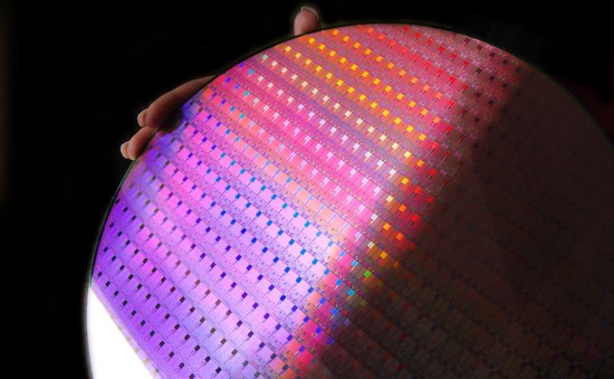
Originally planned to enter mass production in the second half of 2016, Intel’s 10 nm process technology is still barely used by the company today. Currently the process is used to produce just a handful of CPUs, ahead of an expected ramp to high-volume manufacturing (HVM) only later in 2019. Without a doubt, Intel suffered delays on its 10 nm process by several years, significantly impacting the company's product lineup and its business.
Now, as it turns out, Intel’s 10 nm may be a short-living node as the company’s 7 nm tech is on-track for introduction in accordance with its original schedule.
For a number of times Intel said that it set too aggressive scaling/transistor density targets for its 10 nm fabrication process, which is why its development ran into problems. Intel’s 10 nm manufacturing tech relies exclusively on deep ultraviolet lithography (DUVL) with lasers operating on a 193 nm wavelength. To enable the fine feature sizes that Intel set out to achieve on 10 nm, the process had to make heavy usage of mutli-patterning. According to Intel, a problem of the process was precisely its heavy usage of multipatterning (quad-patterning to be more exact).
By contrast, Intel’s 7 nm production tech will use extreme ultraviolet lithography (EUVL) with laser wavelength of 13.5 nm for select layers, reducing use of multipatterning for certain metal layers and therefore simplifying production and shortening cycle times. As it appears, the 7 nm fabrication process had been in development separately from the 10 nm tech and by a different team. As a result, its development is well underway and is projected to enter HVM in accordance with Intel’s unannounced roadmap, the company says.
Murthy Renduchintala, chief engineering officer and president of technology, systems architecture and client group at Intel is quoted to have said at the Nasdaq's 39th Investor Conference:
“7 nm for us is a separate team and largely a separate effort. We are quite pleased with our progress on 7 nm. In fact, very pleased with our progress on 7 nm. I think that we have taken a lot of lessons out of the 10 nm experience as we defined that and defined a different optimization point between transistor density, power and performance and schedule predictability. […] So, we are very, very focused on getting 7 nm out according to our original internal plans.”
The Intel exec reaffirmed the company plans to start HVM production of client CPUs using its 10 nm process technology in 2019, with datacenter products following on a bit later. That said, Intel is clearly not skipping any of its already announced 10 nm products, but implies that its 7 nm products may hit the market earlier than we might expect today (i.e., four years after the 10 nm).
“One thing I will say is that as you look at 7 nm, for us this is really now a point in time where we will get EUV back into the manufacturing matrix, and therefore, I think, that will give us a degree of back to the traditional Moore’s Law cadence that we were really talking about,”
“[With 7 nm] we are going back to more like a 2X scaling factor […] and then really moving forward with that goal.”
Intel has never disclosed characteristics of its 7 nm fabrication tech, but a major reduction of multi-patterning usage as well as a more traditional 2X scaling goal vs. 10 nm indicates a more extensive usage of EUVL.
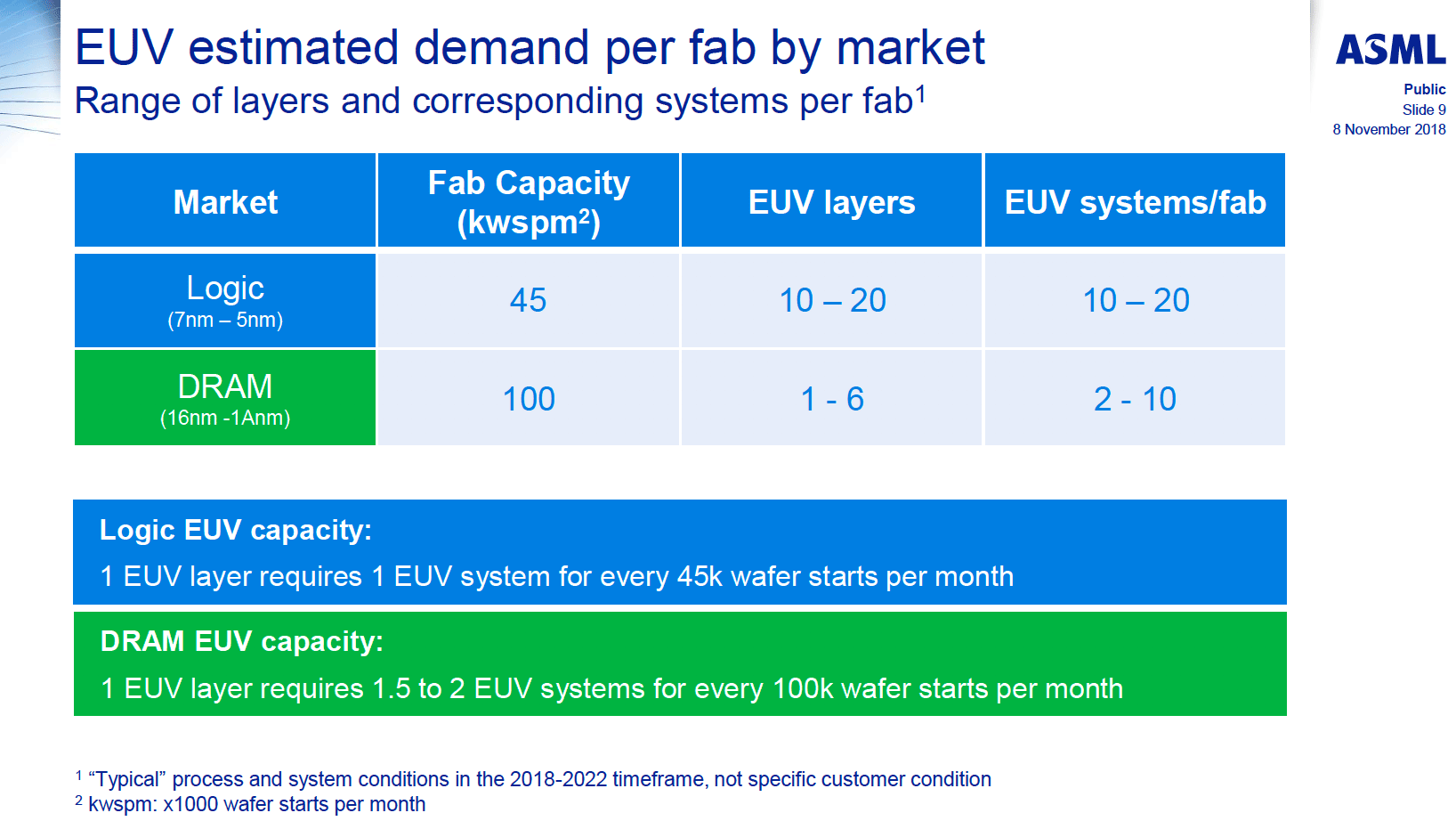
According to ASML, one EUV layer requires one EUV step-and-scan system for every ~45,000 wafer starts per month. Therefore, if Intel plans to use EUVL extensively for 10 to 20 layers, it will require approximately 20 to 40 EUVL scanners for a fab with a 100,000 wafer starts per month capacity. Considering that Intel is not the only company with plans to use EUVL in the 2020s, getting the number of EUVL scanners it might need for HVM at multiple fabs may be a challenge.
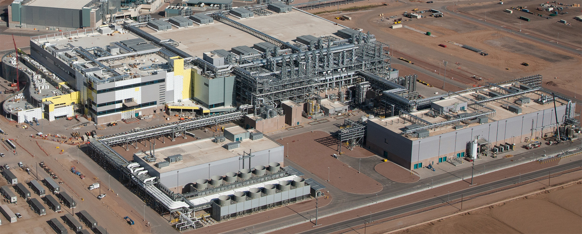
Meanwhile, so far Intel has announced plans for only one 7 nm fab: the Fab 42 in Arizona. In addition, the company is going to have some 7 nm-capable capacity at its D1 facility used for development and trials (among other things).
Related Reading:
- Intel to Equip Fab 42 for 7 nm
- Intel Discloses Plans to Spend $5 Billion on Fab 28 Expansion in Israel
- Intel 10 nm Production Update: Systems on Shelves For Holiday 2019
- Intel’s Xeon Scalable Roadmap Leaks: Cooper Lake-SP, Ice Lake-SP Due in 2020
- Samsung Starts Mass Production of Chips Using Its 7 nm EUV Process Tech
- TSMC: First 7 nm EUV Chips Taped Out, 5 nm Risk Production in Q2 2019
- Samsung Foundry Updates: 8LPU Added, EUVL on Track for HVM in 2019
- ASML Ships Twinscan NXT:2000i Scanner for 7 nm and 5 nm DUV
- EUV Lithography Makes Good Progress, Still Not Ready for Prime Time
Sources: Intel, SeekingAlpha


79 Comments
View All Comments
ajc9988 - Monday, December 17, 2018 - link
Then you didn't dive into AMD's Q3 earnings. CPUs made up 70% of their sales in the consumer segment, with GPUs just 30%. Magically their margins jumped up by like 3 or 4%. Why? Because they have margin left in the tank. On 7nm, the dies per wafer will offset the costs of the wafer easily, which may allow for the leaks going on. First you go for market share, which they have had a windfall due to now having 3x+ what they used to get in server segment (Q4 they are looking at mid-single digits, a bit above 10x the market share they previously had in servers alone), not to mention workstation where Intel's HEDT market got hit decently hard by TR, and mainstream.TSMC 5nm Risk production is Q2, not H2, so you are missing it. 7nm EUV designs are already taped out and volume 5nm is planned for Q2 2020.
Meanwhile Intel's 7nm EUV is late 2021: https://www.eetimes.com/document.asp?doc_id=133365...
Moreover, Intel is making all the right moves NOW. But that fruit won't bear for years.
eastcoast_pete - Monday, December 10, 2018 - link
History did show that Intel hit back with very dirty tricks when the competition (AMD) got uncomfortably close. Intel ended up paying fines for their tactics to blackball AMD from the largest PC manufacturers at the time, but the damage to AMD was done, and AMD almost went under as a result. I hope that this time they hit back the right way, by delivering superior tech with better price/value than AMD. In the meantime, sites like Anandtech can help keeping chipzilla honest by reporting on anything that smells fishy.Targon - Monday, December 10, 2018 - link
You mean that Intel will resort to illegal tactics to stop AMD from gaining market share when AMD has the superior product?Santoval - Friday, December 7, 2018 - link
"And moving to Ice Lake to new 7nm format.."That is certainly not going to happen. Ice Lake is going to be fabbed at 10nm+ and its successor Tiger Lake at 10nm++. Afterwards the picture is unclear. Wikichip still mentions Alder Lake (at 10nm++?) and Meteor Lake (at 7nm), to be released in 2021 and 2022 respectively. However due to Intel's constant delays and the subsequent start of the development of Ocean Cove this will probably be released instead (probably in 2022), either at Intel's last 10nm node or their first 7nm node.
I imagine Intel would like Cove, as their first post-Lake (and even post-Core supposedly) architecture to be fabbed at 7nm. The earliest possible release of Cove, assuming everything goes according to plan, with not a single month of delay either at their fab or design wing, would be in late 2021 - early 2022 (Q4 2019 - Q1 2020 consumer Ice Lake, Q3 to Q4 2020 consumer Tiger Lake and server Ice Lake, no Alder/Meteor Lake release, 2H 2021 server Tiger Lake, and Q4 2021 - Q1 2022 consumer Ocean Cove at either 10nm+++ or 7nm).
This is of course an extremely unrealistic and improbably scenario, which would require all of Intel's lucky stars to perfectly align at the same time. A "2x scaling factor" of 7nm compared to 10nm is still 200+ MTr/mm^2 (million transistors per mm^2), which is simply impossible to do today in anything more than samples due to the immature state of EUV and the low number of EUV scanners. The earliest year I could see Intel releasing 7nm based CPUs in high volume (I'd guess Ocean Cove) is in 2023.
stockolicious - Wednesday, December 12, 2018 - link
That doesn't pass the timing test - If INTC had 7nm ready to go in 2019 what is Raja and Jim Keller doing there? designing for 2025? Raja and Jim have been there less than a year when is anything going to come out with their name on it if they have 7nm and designs aligned for 2019?stockolicious - Wednesday, December 12, 2018 - link
also, it appears INTC is moving full steam ahead in a lot of bold adventures without a CEO and that has been quite some time now. Just a gut feeling but I think they are just marketing now.FreckledTrout - Thursday, December 6, 2018 - link
It's the old bow and arrow management trick. Pull the bow back and fire arrow into the sky. Run up to where the arrow landed in the dirt and paint a bullseye on it. Then proclaim loudly we hit it dead center.HStewart - Thursday, December 6, 2018 - link
Good and expensive management trick, to create a new FAB just for 7nm - no wonder Intel sold the old Micron FAB0ldman79 - Thursday, December 6, 2018 - link
hahahaha!name99 - Friday, December 7, 2018 - link
The ORIGINAL schedule (what they said at IDF13) was 7nm in 2017...