The Qualcomm Snapdragon 855 Pre-Dive: Going Into Detail on 2019's Flagship Android SoC
by Andrei Frumusanu on December 5, 2018 7:00 PM ESTThe new Hexagon 690 now plays an even bigger role
The new Hexagon 690 is both an iteration on past generation units, as well as bringing a totally new aspect to the IP block. The new DSP block doubles up on the number of HVX vector pipelines as compared to the Hexagon 680 and 685 (as a reminder, the 680/685 contained four scalar units along with two 1024b vector processing units). On the scalar pipeline performance, the new unit sees a 20% increase in performance, which might be due to microarchitectural changes or simply a higher clock speed. On the vector side, he new Hexagon now contains four 1024b vector pipelines, doubling the processing power for those units.
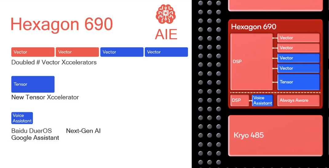
What is entirely new for the new Hexagon IP is the introduction of a new dedicated “tensor accelerator” unit that is seemingly tightly coupled within the larger block. This would most likely be a generally more simplistic MAC array resembling that of other neural network inferencing engines from other vendors. Effectively, this thus represents Qualcomm’s first generation dedicated ML inferencing engine, although Qualcomm does market it as a 4th generation “AI engine” (Previously this nomenclature referred to ML inferencing on CPU, GPU and DSP).
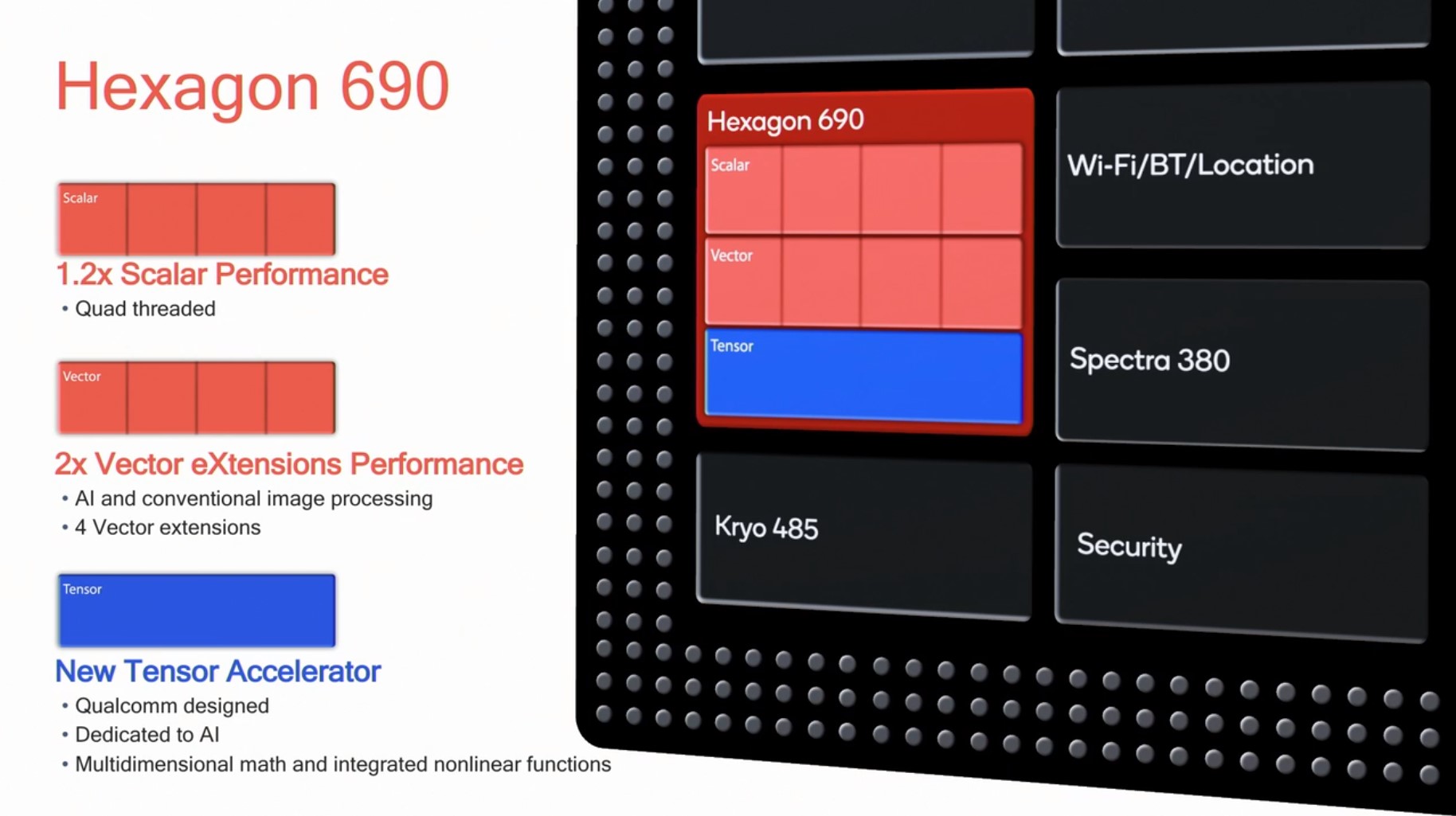
One of the interesting limitations that Qualcomm has wrangled with in previous architectures was that DSP couldn’t process traditional DSP workloads alongside ML inferencing work. However for the S855, Qualcomm has confirmed that the new Tensor units are able to work concurrently and independently alongside the vector units. This means that traditional image processing tasks can now be done in parallel to inferencing tasks, vastly increasing the real-world usability of inferencing on the new Snapdragon platform.
Alongside the vector and tensor units is a new Voice Assistant AI module, designed to accelerate processing for common AI assistants – Qualcomm specifically states Baidu and Google in this case, although it’s unlikely to be exclusive to these two.
New Spectra 380 ISP brings a new Computer Vision accelerator
Alongside the AI Engine, Qualcomm is pairing it with an upgraded Spectra 380 image signalling processor. It also gets a boost to its processing power with a tri-core Computer Vision (CV) ISP. This might seem a little odd – Computer Vision is a family of algorithms that we used to have before the latest advent of machine learning acceleration, so why is it here?
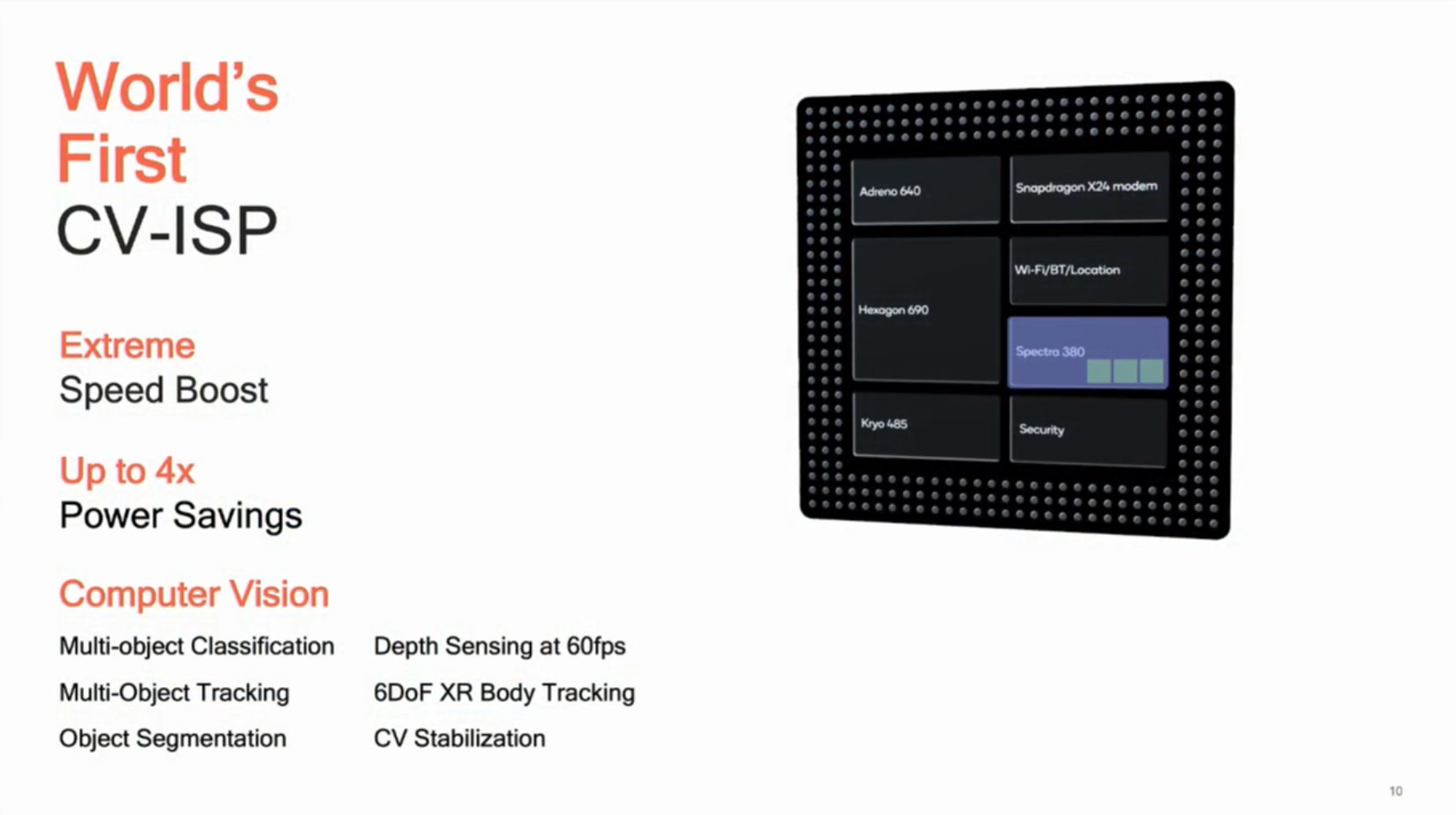
Computer Vision IP is still very useful for various tasks, and in comparison to ML, it's computationally a lot lighter. As such, Qualcomm has deepened its ISP acceleration. With the CV-ISP, Qualcomm believes it can save 4x power (75%?) for image object classification, object segmentation, depth sensing (at 60 FPS), augmented reality body tracking, and image stabilisation.
It’s to be noted that Qualcomm’s claim about being the first computer vision ISP is a bit confusing – it’s definitely not the first SoC with a computer vision IP block, as at least Samsung had this two generations ago. Maybe Qualcomm is referencing some better integration within the ISP pipeline?
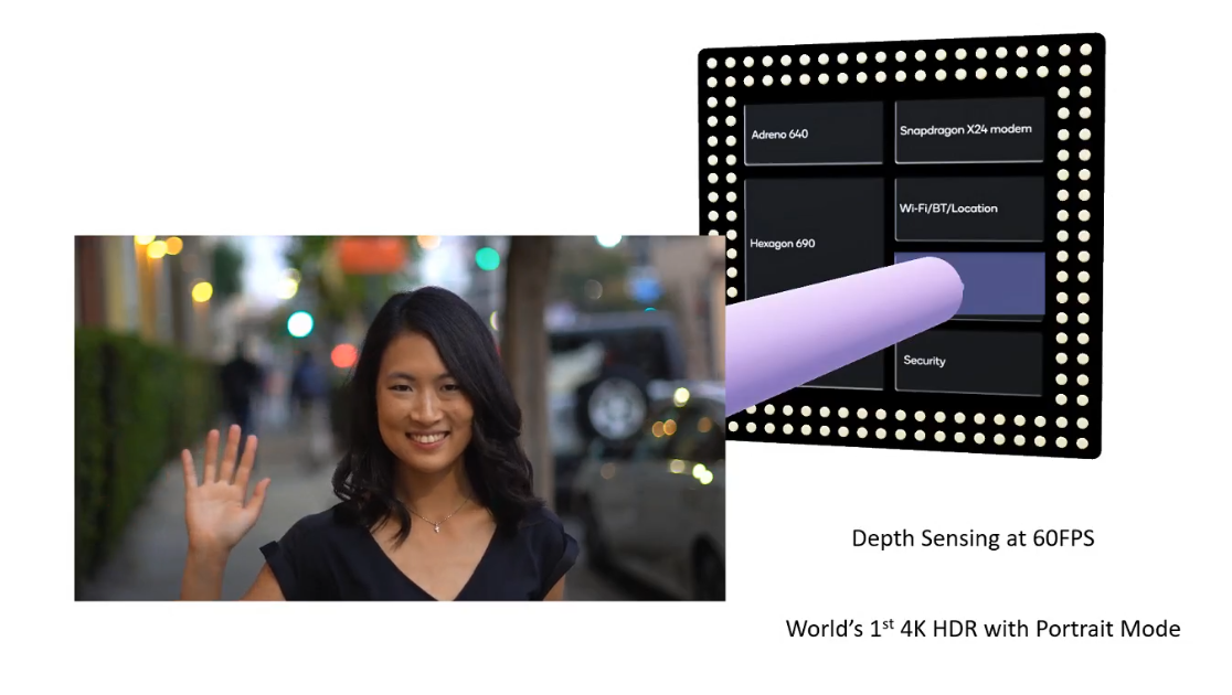
With the new accelerator, Qualcomm states that rather than using the AI Engine for everything, the CV-ISP is preferred for these tasks due to the power savings. The company expects many of the features we normally take for granted in photography will now be available for video as well, such as 4K HDR at 60 FPS with both portrait mode enhancements and depth sensing for live bokeh. Power consumption for 4K HDR capture will be 30% lower than the Snapdragon 845.
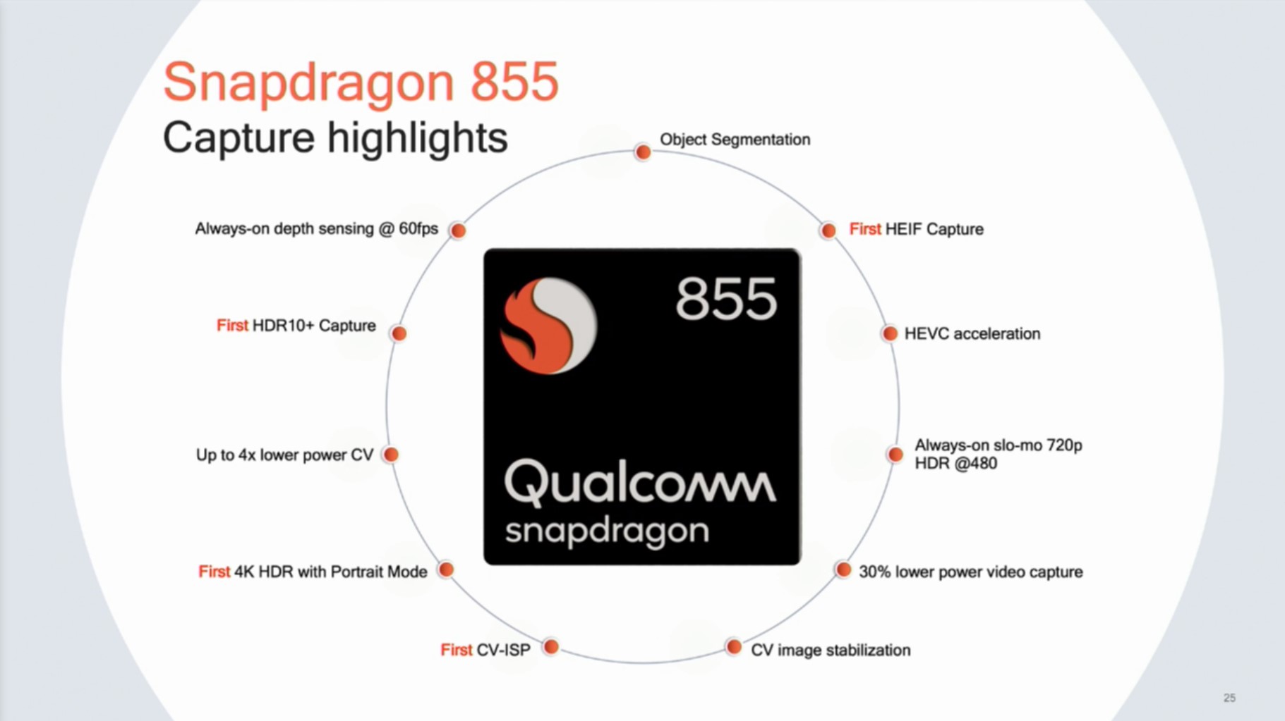
Also in the cards is support for new generations of image formats. Currently JPEG rules the roost in smartphone photography, however the new S855 will support ‘high efficiency image files’, or HEIF, which will offer a large number of new features over JPEG:
- Regular Images Up to 50% Smaller
- HDR Support for multiple color spaces
- Computer Vision data support
- RAW data
- Depth Map support
- Alpha Masking data
- Burst Photography data
- Animated Photography data
- HEVC Video data
The idea here is to enable new use cases for the photos that users take every day. Within the same HEIF, it can store a photo from every camera: a telephoto, a wide angle photo, and a super-wide angle photo for example. This allows of post processing such as bokeh adjustment, object segmentation, quality adjustments, and to a certain extent even basic 3D modelling.
Snapdragon 855 Connectivity
With day one being about Qualcomm’s approach to 5G, connectivity is going to be at the heart of the S855. Built into the chip is the Snapdragon X24 modem, which offers LTE Category 20 class download speeds good for up to 2 Gbps on supported devices and networks. The increased speeds are achieved by using up to 7x carrier aggregation with 4x4 MIMO and 256QAM. On the upload side, the new SoC modem now also for the first time supports 256QAM, able to double the peak upload rate to up to 300Mbps with 3xCA.
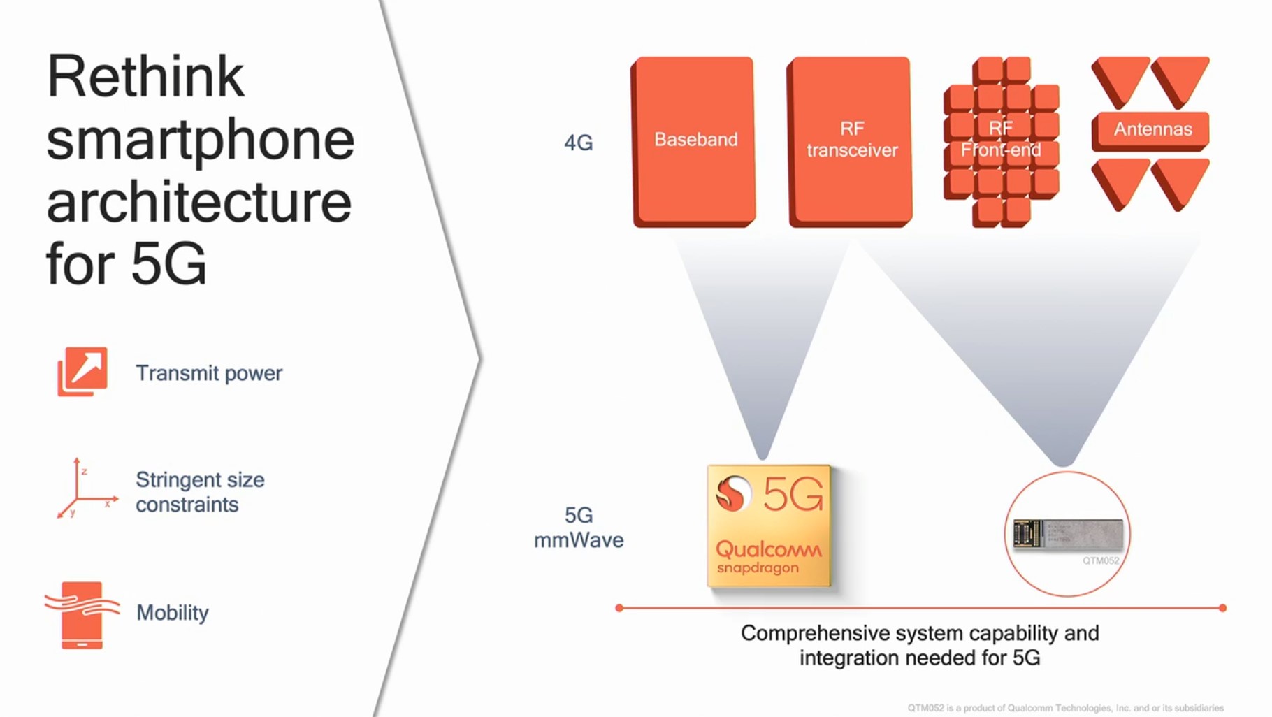
Meanwhile when it comes to 5G, for the S855 platform it’s not the actual SoC which delivers this, but rather the external Snapdragon X50 modem. When combined with the S855, the platform will support both mmWave (>24 GHz) and sub-6 GHz 5G NR technologies. Qualcomm made mention of its entrance in the RFFE (RF front-end) field, which the company now includes in its QTM052 RFFE/antenna mini modules.

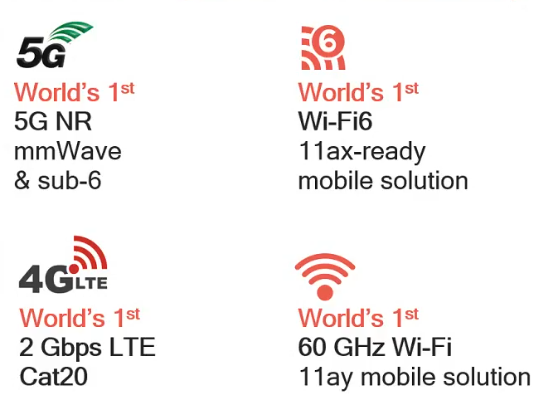
Not to be left behind, Qualcomm has also improved their local wireless networking capabilities as well. Snapdragon 855 support of the new WiFi 6 standard (802.11ax) as well as the new 60GHz “Wi-Gig” 802.11ay standard, enabled by an external WiFi combo chipset.
First impressions
Overall the new Snapdragon 855 promises some great improvements in pretty much every single aspect of the SoC. The biggest generational improvements seem to be on the CPU side, where Qualcomm promises a 45% jump in performance. The figure is pretty much in line with what we’ve seen on the Kirin 980, and that SoC performed excellently. And I’m certain Qualcomm will be able to squeeze out even more performance through software.
One big uncertaintly that I have is in regards to the CPU configuration. Here at first I thought the 1+3 configuration seemed reasonable, however the disclosure that the different cores are running on the same power/voltage plane has given me some doubts about how this will pan out in terms of power efficiency. Power efficiency of the CPU and the SoC in general use-cases seems to be something that Qualcomm hasn’t talked about at all today and this worries me quite a bit.
On the GPU side, as expected the new Adreno 640 is just an iterative design on the Adreno 630 – increasing the number of ALUs versus its predecessor by 50%. The performance gains were quoted at 20%, which are a bit on the conservative side but not something to be particularly worried about. Power efficiency is claimed to still be leading edge, and at least based on the sustained performance metrics showed it looks like the Snapdragon 855 will continue to lead in this regard.
The Snapdragon 855 is Qualcomm’s first chipset to include a dedicated neural network inference engine / “NPU”. Here Qualcomm claims to have a lead over its nearest competitor, the Kirin 980, however it’s something that will need a thorough investigation in the future, as we’ve seen that both vendors' software stacks aren’t quite mature enough to be able to fully extract the capabilities of the hardware. Still, this is an important step for Qualcomm as it now allows concurrent usage of the DSP for image processing while having a dedicated hardware block for inferencing tasks.
The ISP and the new computer vision hardware seem fantastic, the new features are really raising the bar in what will be possible with computational photography as well as introduce new aspects such as computational videography. Here we’ll have to see what OEM vendors will be able to actually implement on final commercial devices.
Last but not least, the Snapdragon 855 is the first platform that promises to provide a complete solution of next generation connectivity technologies. Here the features aren’t directly featured into the SoC but rather in accompanying chipsets, so I do expect that there’s going to be many devices that will not chose the full set of next-generation solutions, but also we might see some devices which will implement the new X50 5G modem alongside the new WiFi6/.11ax and 11ay WiFi solutions.
Today’s announcement is just the first wave of information on the Snapdragon 855. To really judge the new chipset, we’re eagerly waiting on Qualcomm to allow us to do a performance preview on the reference designs. Most importantly, we’re still a few months away from the first commercial devices – which will represent the definitive evaluation of the new chipset.


47 Comments
View All Comments
tyger11 - Wednesday, December 5, 2018 - link
With this generation of mobile SoCs, I'm finally getting pretty curious as to how these compare with typical workloads to regular desktop CPUs. Being able to handle 4K60p encode and decode, etc, means that these have gotta be powerful enough for 99% of the every day uses most people have. Putting them in cases with decent cooling (as opposed to a severely thermally-constrained situation like a cellphone or even a tablet) has really gotta be a very nice solution for a lot of people. Or just dock your phone with something like the DeX.HStewart - Wednesday, December 5, 2018 - link
I often thought about that - especially I wonder if it take hardware to movie pixels more on say a 28in screen than a 7in screen even at same resolution.Just for information I have Note 8 with DeX and it not that impressive. Of Samsung wants you get a Note 9.
Death666Angel - Thursday, December 6, 2018 - link
"if it take hardware to movie pixels more" What?And the physical size of the pixels is not important to the device supplying the picture.
4k60 encode / decode does not have anything to do with general performance, those are fixed function blocks in the chips.
Although I'm also curious how they would perform in general windows tasks against a variety of laptop and desktop CPU solutions. It's a shame hardly any ARM based solutions outside of smartphones are price competitive against Intel Atom, Core or AMD stuff. Snapdragon 835 / 845 laptops with Windows mode S (I think that's what it's called) going for $800 and more is ridiculous.
jasonslg - Wednesday, December 5, 2018 - link
For the performance part of the problem, I just found a small interview with Travis Lanier, senior director of product management at Qualcomm, and asked a few questions that everyone should be interested in.1.L2 of 855 is 512KB 256KB 128KB, L3 2MB, system cache 3MB
2.Adreno640 adds 50% alu, using AI
3.Trepn profiler no longer maintains
4.The peak power consumption of 855 and 845, no specific value, only indicates almost
halcyon - Thursday, December 6, 2018 - link
Gy!halcyon - Thursday, December 6, 2018 - link
I mean Thank You (really need that 5minute edit time window in 2018, @AnandTech).jasonslg - Thursday, December 6, 2018 - link
not me . I just quote media reports.Ian Cutress - Thursday, December 6, 2018 - link
I've been speaking with him today and I got a few more details. Update when I can get a few minutes in front of my laptop.tipoo - Thursday, December 6, 2018 - link
re: The Prime core being on the same power domain as the other three big cores, though that's not as ideal as it could have been, the other cores waking up doesn't mean they're at max power doing so, right?Zoolook13 - Friday, December 7, 2018 - link
No not max power, but they are probably at a higher voltage level than they would need to be on, so consuming more power than they would if they had a separate power plane.