AMD Announces Radeon Instinct MI60 & MI50 Accelerators: Powered By 7nm Vega
by Ryan Smith on November 6, 2018 4:00 PM EST- Posted in
- GPUs
- AMD
- Enterprise
- Machine Learning
- Vega
- AMD Instinct

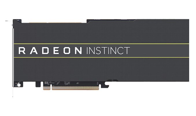
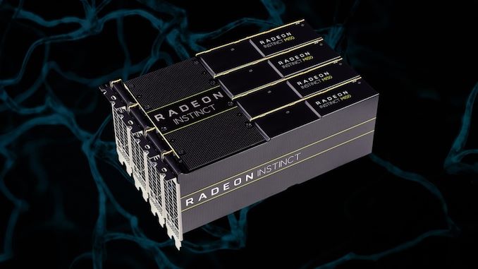
As part of this morning’s Next Horizon event, AMD formally announced the first two accelerator cards based on the company’s previously revealed 7nm Vega GPU. Dubbed the Radeon Instinct MI60 and Radeon Instinct MI50, the two cards are aimed squarely at the enterprise accelerator market, with AMD looking to significantly improve their performance competitiveness in everything from HPC to machine learning.
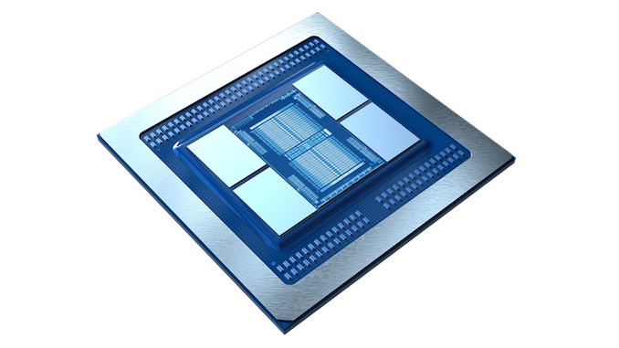
Both cards are based on AMD’s 7nm GPU, which although we’ve known about at a high level for some time now, we’re only finally getting some more details on. GPU is based on a refined version of AMD’s existing Vega architecture, essentially adding compute-focused features to the chip that are necessary for the accelerator market. Interestingly, in terms of functional blocks here, 7nm Vega is actually rather close to the existing 14nm “Vega 10” GPU: both feature 64 CUs and HBM2. The difference comes down to these extra accelerator features, and the die size itself.
With respect to accelerator features, 7nm Vega and the resulting MI60 & MI50 cards differentiates itself from the previous Vega 10-powered MI25 in a few key areas. 7nm Vega brings support for half-rate double precision – up from 1/16th rate – and AMD is supporting new low precision data types as well. These INT8 and INT4 instructions are especially useful for machine learning inferencing, where high precision isn’t necessary, with AMD able to get up to 4x the perf of an FP16/INT16 data type when using the smallest INT4 data type. However it’s not clear from AMD’s presentation how flexible these new data types are – and with what instructions they can be used – which will be important for understanding the full capabilities of the new GPU. All told, AMD is claiming a peak throughput of 7.4 TFLOPS FP64, 14.7 TFLOPS FP32, and 118 TOPS for INT4.
7nm Vega also buffs up AMD’s memory capabilities. The GPU adds another pair of HBM2 memory controllers, giving it 4 in total. Combined with a modest increase in memory clockspeeds to 2Gbps, and AMD now has a full 1TB/sec of memory bandwidth in the GPU’s fastest configuration. This is even more than NVIDIA’s flagship GV100 GPU, giving AMD the edge in bandwidth. Meanwhile as this is an enterprise-focused GPU, it offers end-to-end ECC, marking the first AMD GPU to offer complete ECC support in several years.
The enterprise flourishes also apply to 7nm Vega’s I/O options. On the PCIe front, AMD has revealed that the GPU supports the recently finalized PCIe 4 standard, which doubles the amount of memory bandwidth per x16 slot to 31.5GB/sec. However AMD isn’t stopping there. The new GPU also includes a pair of off-chip Infinity Fabric links, allowing for the Radeon Instinct cards to be directly connected to each other via the coherent links. I’m still waiting for a confirmed breakdown on the numbers, but it looks like each link supports 50GB/sec down and 50GB/sec up in bandwidth.
Notably, since there are only 2 links per GPU, AMD’s topology options will be limited to variations on rings. So GPUs in 4-way configurations won’t all be able to directly address each other. Meanwhile AMD is still sticking with PCIe cards as their base form factor here – no custom mezzanine-style cards like NVIDIA – so the cards are connected via a bridge on the top. Meanwhile backhaul to the CPU (AMD suggests an Epyc, of course) is handled over PCIe 4.
Finally, looking at the GPU itself, it’s interesting to note just how small it is. Because AMD didn’t significantly bulk up the GPU on CUs, thanks to the 7nm process the new GPU is actually a good bit smaller than the original 484mm2 Vega 10 GPU. The new GPU comes in at 331mm2, packing in 13.2B transistors. Though it should be noted that AMD’s performance estimates are realistically conservative here; while 7nm does bring power consumption down, AMD is still only touting >1.25x performance of MI25 at the same power consumption. The true power in the new cards lies in their new features, rather than standard FP16/FP32 calculations that the existing MI25 card was already geared for.
Wrapping things up, Radeon Instinct MI60 will be shipping in Q4 of this year. AMD has not announced a price, but as a cutting-edge 7nm GPU, don’t expect it to be cheap. MI60 will then be followed by MI50 in Q1 of next year, giving AMD’s customers a second, cheaper option to access 7nm Vega.
Source: AMD


26 Comments
View All Comments
Yojimbo - Saturday, November 10, 2018 - link
By the way, here is Resnet-50 training using the latest NVIDIA toolchain and the Tensor Cores on their GPUs:http://3s81si1s5ygj3mzby34dq6qf-wpengine.netdna-ss...
wingless - Tuesday, November 6, 2018 - link
Infinity Fabric has more bandwidth than NVLink for the GPU to GPU connections. That's an interesting tidbit. I hope this quickly trickles down into consumer cards like it did the Nvidia RTX line. I want to see some shared-memory Crossfire configurations ASAP.pSz - Tuesday, November 6, 2018 - link
That's not correct. On the V100 NVIDIA has up to 3x 50 GB/s bi-directional links, so that's 150 / 150 Gb/s up/down link (which they refer to as 300 GB/s) in the SXM2 packaging, see [1]. The PCIe boards AFAIK do not have NVLink connectors; the Quadro GV100's however do have two per board [2], hence can communicate with 100/100 GB/s max.It will be interesting to see how flexible are the topologies AMD will allow and how will those connectors be implemented in dense configurations where as in many applications you can't afford 5U of rackspace just to place cards vertically next to each other for the rigid connectors that they picture.
[1] https://www.nvidia.com/en-us/design-visualization/...
[2] https://www.nvidia.com/en-us/design-visualization/...
p1esk - Tuesday, November 6, 2018 - link
2080Ti has NVLink (100GB/s).Yojimbo - Tuesday, November 6, 2018 - link
The 2080 Ti only has 2 NVLink connectors. But why would you compare the MI60 to the 2080Ti rather than the Tesla V100?skavi - Wednesday, November 7, 2018 - link
How reasonable is a chiplet design for GPUs? I can speculate on this myself, so please only answer if you have real insight.abufrejoval - Wednesday, November 7, 2018 - link
I guess it's important to remember that this is a cloud design and meant to be shared, for scale in and scale out.For scale out, it won't be used as a gaming accellerator, but HPC accellerator, where no GPU would ever be big enough anyway. Having fixed (or at least order of 2) sizes makes it less of an effort to tune (and schedule) the HPC applications across the racks.
For scale-in, that is VMs or containers with fractional parts of these chiplets: It makes a lot of sense to hit something that gives you good FHD performance and then profit from the lower cost and higher yields of the smaller chips.
I would think that yields on EUV are much better with smaller chips and AMD is teaching Intel and Nvidia a lesson about bigger chips not necessarily being the smarter solution and that you need to connect properly: Lisa makes it personal :-)
abufrejoval - Wednesday, November 7, 2018 - link
Failed to mention: Scale in is where I see them hitting the new cloud gaming target.haukionkannel - Wednesday, November 7, 2018 - link
Maybe in future some cpu IO gpu combination... and then only maybe. The separate IO part reduce the speed somewhat compared to monolith.Multi gpu has one big problem. The operation systems does not support multi gpu system directly. You have to write separate drivers to each applications like in sli and crossfire. Osses has supported directly multible cpu a long time so They just work because the os distributes the tasks to different CPUs. We need similar support to os so that it can directly use multible GPUs without manual handling.
edzieba - Wednesday, November 7, 2018 - link
Somewhat. OSes have support for multiple homogenous cores with the same access to IO memory etc. Support for multiple heterogeneous CPUS (e.g. multiple sockets, CPUs with internal NUMA domains) is in the same "technically present but requires explicit implementation to actually work with any utility" as multiple GPUs.