AMD Unveils ‘Chiplet’ Design Approach: 7nm Zen 2 Cores Meet 14 nm I/O Die
by Anton Shilov on November 6, 2018 1:53 PM EST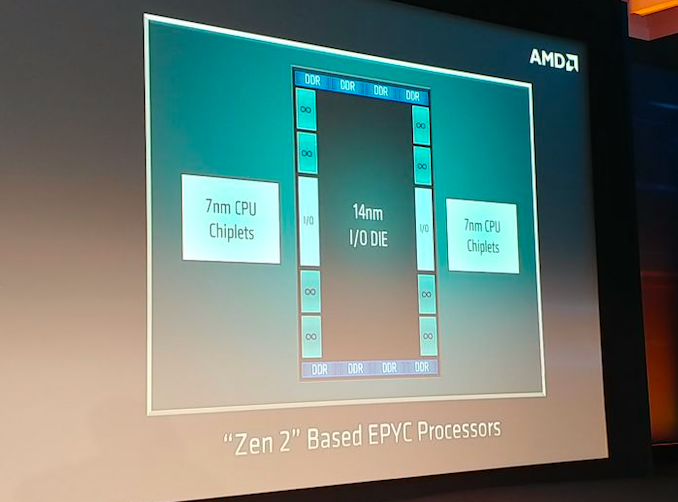
AMD on Tuesday disclosed some additional details about its upcoming codenamed Rome processor based on its Zen 2 microarchitecture. As it turns out, the company will use a new design approach with its next-generation EPYC CPUs that will involve CPU ‘chiplets’ made using TSMC’s 7 nm manufacturing technology as well as an I/O die made using a 14 nm fabrication process.
AMD’s chiplet design approach is an evolution of the company’s modular design it introduced with the original EPYC processors featuring its Zen microarchitecture. While the currently available processors use up to four Zen CPU modules, the upcoming EPYC chips will include multiple Zen 2 CPU modules (which AMD now calls ‘chiplets’) as well as an I/O die made using a mature 14 nm process technology. The I/O die will feature Infinity Fabrics to connect chiplets as well as eight DDR DRAM interfaces. Since the memory controller will now be located inside the I/O die, all CPU chiplets will have a more equal memory access latency than today’s CPU modules. Meanwhile, AMD does not list PCIe inside the I/O die, so each CPU chiplet will have its own PCIe lanes.
Separating CPU chiplets from the I/O die has its advantages because it enables AMD to make the CPU chiplets smaller as physical interfaces (such as DRAM and Infinity Fabric) do not scale that well with shrinks of process technology. Therefore, instead of making CPU chiplets bigger and more expensive to manufacture, AMD decided to incorporate DRAM and some other I/O into a separate chip. Besides lower costs, the added benefit that AMD is going to enjoy with its 7 nm chiplets is ability to easier bin new chips for needed clocks and power, which is something that is hard to estimate in case of servers.
This is a breaking news. We are updating the news story with more details.
Source: AMD


76 Comments
View All Comments
MagpieSVK - Wednesday, November 7, 2018 - link
Maybe they will create 2 Channel 2 infinity fabric interconnect IO chip and use it with 2 chiplets in R7 series and with one chiplet one GPU on APU lineupTargon - Wednesday, November 7, 2018 - link
The real beauty of the approach that AMD is taking is that they can scale the design and evolve things well. Those Zen2 cores for example tie into the IO "module", but the IO module itself can be updated and get different configurations based on the target processor, socket, or whatever. Since AMD has supported Gen-Z consortium, I expect that all of this will come together in 2020 or 2021 where the need for dedicated PCI Express lanes on the CPU won't be needed, because those will hang off the Gen-Z bus, and all of those pins currently used for PCI Express support can then be used to tie into Gen-Z for a LOT of bandwidth.jmnewton - Wednesday, November 7, 2018 - link
I'm pretty sure the IO Pins are just generic high-speed SERDES that can internally be routed to control logic for IF 2.0, PCIe 4, GenZ, OpenCAPI, NVMe direct, USB 3.2, Ethernet, etc. If you look at many chipsets from Intel, AMD the motherboard implementation dictates which control logic gets connected to that physical port. Sometimes it can be bifurcated (think: (1) 16x PCIe 4.0 port or 1 8x PCIe 4.0 port + 2 USB 3.2 ports, etc).It will be very interesting to see what options they do have for the IO die and its configurability.
I also think they might use some similar kinds of MCM setups for a set of Zen2 dies with a set of Radeon dies. Imagine 2 Zen2 dies + a decent Radeon die (or 2) and you've got a pretty nice workstation part. Your "APU" now becomes a mix-n-match game between the 2 sets of dies.
Azix - Thursday, January 10, 2019 - link
Does not listing PCI-e mean that each chiplet will have its own lanes? Isn't PCI-e I/O? Isn't that almost all the I/O in PCs nowadays?