AMD Unveils ‘Chiplet’ Design Approach: 7nm Zen 2 Cores Meet 14 nm I/O Die
by Anton Shilov on November 6, 2018 1:53 PM EST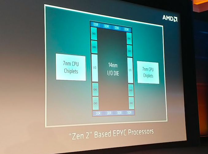
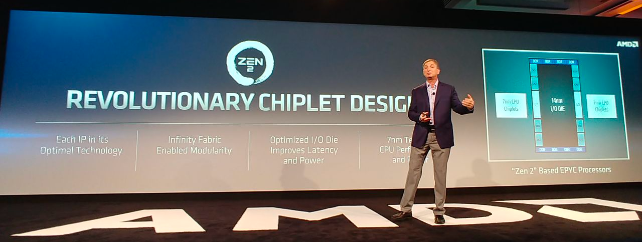
AMD on Tuesday disclosed some additional details about its upcoming codenamed Rome processor based on its Zen 2 microarchitecture. As it turns out, the company will use a new design approach with its next-generation EPYC CPUs that will involve CPU ‘chiplets’ made using TSMC’s 7 nm manufacturing technology as well as an I/O die made using a 14 nm fabrication process.
AMD’s chiplet design approach is an evolution of the company’s modular design it introduced with the original EPYC processors featuring its Zen microarchitecture. While the currently available processors use up to four Zen CPU modules, the upcoming EPYC chips will include multiple Zen 2 CPU modules (which AMD now calls ‘chiplets’) as well as an I/O die made using a mature 14 nm process technology. The I/O die will feature Infinity Fabrics to connect chiplets as well as eight DDR DRAM interfaces. Since the memory controller will now be located inside the I/O die, all CPU chiplets will have a more equal memory access latency than today’s CPU modules. Meanwhile, AMD does not list PCIe inside the I/O die, so each CPU chiplet will have its own PCIe lanes.
Separating CPU chiplets from the I/O die has its advantages because it enables AMD to make the CPU chiplets smaller as physical interfaces (such as DRAM and Infinity Fabric) do not scale that well with shrinks of process technology. Therefore, instead of making CPU chiplets bigger and more expensive to manufacture, AMD decided to incorporate DRAM and some other I/O into a separate chip. Besides lower costs, the added benefit that AMD is going to enjoy with its 7 nm chiplets is ability to easier bin new chips for needed clocks and power, which is something that is hard to estimate in case of servers.
This is a breaking news. We are updating the news story with more details.
Source: AMD


76 Comments
View All Comments
drunkenmaster - Wednesday, November 7, 2018 - link
I/O goes both ways, there are two ends to a connection and two signals being made. Also that assumes no improvements to the process, optimisations to the IF controller design and optimisations in terms of how communication is routed and how far the signals go thus which all individually change the power usage of the i/o. Even pci-e 4 should improve efficiency and thus power usage for IF.More importantly maybe, for a given number of wafer starts, if you can move over half the die to 14nm, then even if it increases power, it can double the amount of chips you can produce. Seeing as the chip coming looks like it will trash anything Intel can produce in server handily with vastly higher performance per watt and that will be true through to at least early 2020(minimum) then AMDs biggest issue will in fact be volume, not power.
This will both allow AMD to produce more EPYCs and then as capacity increases and they get more wafer starts it means they can get more 7nm gpus and desktop cpus/apus all done on 7nm sooner if those wafers aren't required for EPYC.
Not to mention that the massively increased yields from splitting off the cores from uncore and the i/o once again increases potential chips being produced.
GreenReaper - Wednesday, November 7, 2018 - link
On the plus side, if it's in the center it'll presumably get the most benefit from the cooling, and it'll make good use of the rest of the area if each core has its own space (and as you say, they may not need as much power, so use less cooling capacity).EasyListening - Thursday, November 15, 2018 - link
I heard Vega scales down to 8W quite nicelyMrSpadge - Tuesday, November 6, 2018 - link
Besides the limited scaling of interfaces with process nodes, you could use different processes tuned for lower power in a dedicated I/O chip. Not sure what is done and needed here, but there may actually be power benefits to this.PeachNCream - Tuesday, November 6, 2018 - link
I hope so. I'm also hoping that a centralized IF results in lower inter-core latency and lower memory latency in high core count products. Honestly, this design change looks a bit like a star topology and less like a mesh. I'd love to see some testing done to see what portion of the total TDP will get spent by the IF/DRAM die.jospoortvliet - Wednesday, November 7, 2018 - link
I would expect that the entire reason they have done this is precisely to decrease the amount of energy spend on fabric. They surely are very much aware of that problem and this star topology and big ram cache might help a lot... At least I hope for them that that is the case ;-)jjj - Tuesday, November 6, 2018 - link
Having an IO die allows one to optimize for IO so they will have lower power than with integrated on 7nm - when integrated, you can't afford to optimize for IO as other blocks are much more important.looncraz - Wednesday, November 7, 2018 - link
Power usage is my main concern with this design.I believe AMD will use dynamic IF frequency like Vega does. This will allow links to slow down to, say, 800MHz or even shut down when not in use or when load is not high. Otherwise idle power will be insane since the IF also needs to be running MUCH faster than on Summit/Pinnacle Ridge to supply the bandwidth required.
Spunjji - Friday, November 9, 2018 - link
This is a server chip, so while idle power isn't entirely irrelevant it's still not their biggest priority. After all, if you've paid to deploy and run a server that's not doing anything then you're pouring money down the drain.abufrejoval - Wednesday, November 7, 2018 - link
I/O amplifiers require surface area or actually volume I guess, so all those amps that power external off-chip lines to DRAM, PCIe slots they are big by necessity, somewhat like high-voltage long distance power lines vs. the wiring inside your house. It's one of the reasons that they do/did HBM stack base dies and silicon interposers on 65nm nodes, because there is no benefit to going small and the equipment was still around.And even if the surface area is larger, that makes for better cooling, too.
Two hundred watts on the surface of you pinky's fingernail is a bit of a bother, same wattage on the size of a credit card, much less of a problem.