TSMC: First 7nm EUV Chips Taped Out, 5nm Risk Production in Q2 2019
by Anton Shilov on October 9, 2018 4:00 PM EST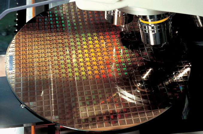
Last week, TSMC made two important announcements concerning its progress with extreme ultraviolet lithography (EUVL). First up, the company has successfully taped out its first customer chip using its second-generation 7 nm process technology, which incorporates limited EUVL usage. Secondly, TSMC disclosed plans to start risk production of 5 nm devices in April.
First 7 nm EUV Chip Tapes Out at TSMC
TSMC initiated high-volume manufacturing of chips using its first generation 7 nm fabrication process (CLN7FF, N7) in April. N7 is based around deep ultraviolet (DUV) lithography with ArF excimer lasers. By contrast, TSMC’s second-generation 7 nm manufacturing technology (CLN7FF+, N7+) will use extreme ultraviolet lithography for four non-critical layers, mostly in a bid to speed up production and learn how to use ASML’s Twinscan NXE step-and-scan systems for HVM. Factual information on the improvements from N7 to N7+ are rather limited: the new tech will offer a 20% higher transistor density (because of tighter metal pitch) and ~8% lower power consumption at the same complexity and frequency (between 6% and 12% to be more precise).
While the advantages of N7+ over its predecessors are not significant (e.g., TSMC has never mentioned performance increases that the new tech is expected to bring), it will still almost certainly be embraced wholeheartedly by developers of mobile SoCs who need to release new chips every year. That said, it is not surprising that TSMC has already taped out the first chip using its N7+ technology. Furthermore, the company is prepping a specialized version of N7 process aimed at the automotive industry, which indicates that N7/N7+ is going to be a “long” node.
TSMC is not disclosing the name of the customer whose N7+ SoC it has taped out, but considering the foundry’s alpha customers for new process technologies in the recent years, the leading suspects are obvious.
| Advertised PPA Improvements of New Process Technologies Data announced by companies during conference calls, press briefings and in press releases |
||||||||
| TSMC | ||||||||
| 16FF+ vs 20SOC |
10FF vs 16FF+ |
7FF vs 16FF+ |
7FF vs 10FF |
7FF+ vs 7FF |
5FF vs 7FF |
|||
| Power | 60% | 40% | 60% | <40% | 10% | 20% | ||
| Performance | 40% | 20% | 30% | ? | same (?) | 15% | ||
| Area Reduction | none | >50% | 70% | >37% | ~17% | 45% | ||
5 nm on Track
After N7+ comes TSMC’s first-generation 5 nm (CLN5FF, N5) process, which will use EUV on up to 14 layers. This will enable tangible improvements in terms of density, but will require TSMC to extensively use EUV equipment. When compared to TSMC’s N7, N5 technology will enable TSMC's customers to shrink area of their designs by ~45% (i.e. transistor density of N5 is ~1.8x higher than that of N7), increase frequency by 15% (at the same complexity and power) or reduce power consumption by 20% power reduction (at the same frequency and complexity).
TSMC will be ready to start risk production of chips using its N5 tech in April, 2019. Keeping in mind that it typically takes foundries and their customers about a year to get from risk production to HVM, it seems like TSMC is on-track for mass production of 5 nm chips in Q2 2020, right in time to address smartphones due in the second half of 2020.
EDA tools for the N5 node will be ready in November, so chip designs may be well underway now. But while many foundation IP blocks for N5 are ready today, there are important missing pieces, such as PCIe Gen 4 and USB 3.1 PHYs, which may not be ready until June. For some of TSMC's clients the lack of these pieces is not a problem, but many will have to wait.
One of the factors that prevents smaller companies from designing FinFET chips is development cost. Some estimates put the average cost to develop an SoC at around $150 million in labor and IP licenses. With N5 generation, these expenditures will rise to $200 – $250 million, according to EETAsia, which will limit the number of parties interested in using the tech.
Related Reading:
- TSMC Details 5 nm Process Tech: Aggressive Scaling, But Thin Power and Performance Gains
- TSMC Starts to Build Fab 18: 5 nm, Volume Production in Early 2020
- AMD's 7nm CPUs & GPUs To Be Fabbed by TSMC, on Track for 2018 - 2019
- TSMC Kicks Off Volume Production of 7nm Chips
Source: EETAsia


50 Comments
View All Comments
overseer - Wednesday, October 10, 2018 - link
Very likely, given a rumored 2021 PS5 launch. Even 7FF can be quite durable, and just slightly weaker than 7FF+.gfkBill - Tuesday, October 9, 2018 - link
"which indicates that N7+ is going to be a “long” node." - I haven't come across that, in spite of being an avid Anand and Ars reader - long life? Google isn't helping much."the leading suspects are obvious." - would it have killed you to mention them? Just sounds snobby leaving it hanging like that.
aryonoco - Tuesday, October 9, 2018 - link
Long life, a node that will have a longer lifespan. Compare TSMC's 28nm vs 20nm. Or their 16nm vs their 10nm.Usual suspects are Apple and Huawei (HiSilicon).
name99 - Wednesday, October 10, 2018 - link
"long node" and "short node" are terms of insult, not terms of information...iwod is correct. Nodes (at least for fabs) last effectively forever. Look at TSMC, they're still offering .13µ if you want that, and terms that were claimed as "short nodes" at the time, like 20nm, are still doing just fine.
To the extent that "short node" means ANYTHING, it means that it won't last long AS THE LEADING EDGE. ie there's a kind of cadence that some nodes stay leading edge for one year (20 nm, 10 nm), some stay leading edge for two years (16nm, 7nm).
Does this prove anything other than "three does not divide into two exactly"? Not really. But if you're in the business of trying to talk down the fabs (or their customers), you latch onto whatever nonsense you can. "short node" sounds bad --- must imply a weakness of some sort, no? Hence a whole lot of idiotic chatter around how TSMC 20nm or 10nm (or its client parts, like the relevant Apple chips) were going to suck.
Basically exactly the same phenomenon as when people who know nothing about finance feel educated and entitled to an opinion by hearing that an exchange rate is "strong".
iwod - Tuesday, October 9, 2018 - link
TSMC and Apple has been working together on leading node for a few years now. So both Roadmap are perfectly aligned with each other. 7nm+ for 2019 iPhone, and 5nm for 2020 iPhone."Long Node" simply means a node./ Fab tech won't be discontinued soon. 10nm are short node. TSMC provides an upgrade path where customer on 28nm can upgrade to 20nm > 12nm > 7nm when they see fits. Long node also usually means they are cost optimised and constantly being refined and improved, for TSMC that is cheaper to produce, and in the long run cheaper for customer to use.
Speedfriend - Wednesday, October 10, 2018 - link
Everything have seen indicates that N7+ is going to be a short node, as its sole purpose is to getting the EUV scanner working for 5nm. And also that Apple is not going to use it, but is going to use 7nm twice and then 5nmIJD - Wednesday, October 10, 2018 - link
2018 iPhone uses N7, 2019 will use N7+, 2020 will use N5 -- you can see that TSMC's mass production schedules perfectly line up with Apple's. The reason is increasing gate density means cheaper chips, or more functionality/features for the same cost chip -- this is true even with rising wafer cost, gate density still increases faster than wafer cost.hechacker1 - Thursday, October 11, 2018 - link
Just thinking what a beast of an iPhone or iPad will best at 2020. It absolutely will be able to replace a Mac.edzieba - Wednesday, October 10, 2018 - link
Same as TSMC's 16nm, which was turned into 16FF, 16FF+, 16FFC, 12FFC, and 12FFN over the last 4 years (and you could even call 16nm a varaint of 20nm if you were feeling uncharitable).Anymoore - Tuesday, October 9, 2018 - link
It was also reported 5nm EUV needed multipatterning (same as current 7nm). So 7nm+ probably needs same amount of multipatterning as 10nm. It's unlikely there are enough EUV tools for the same volume as before.