16GB NVIDIA Tesla V100 Gets Reprieve; Remains in Production
by Ryan Smith on May 24, 2018 8:00 PM EST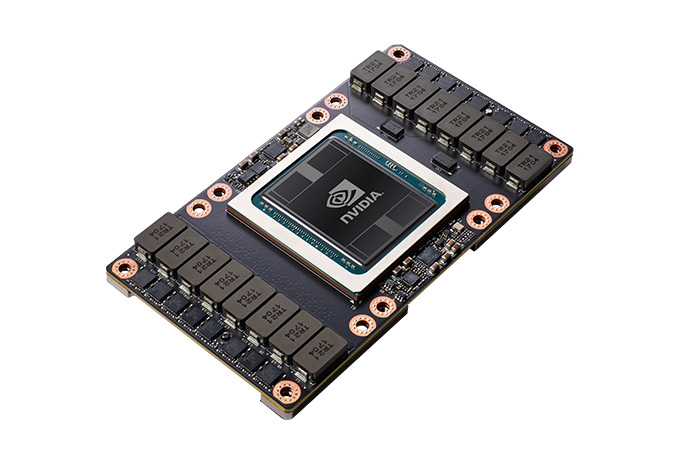
Back in March at their annual GPU Technology Conference, NVIDIA announced the long-anticipated 32GB version of their flagship Tesla V100 accelerator. By using newer 8-Hi HBM2 memory stacks, NVIDIA was able to double the accelerator’s previous 16GB of VRAM to a class-leading 32GB. Meanwhile, at the time company representatives told us that the launch of the 32GB model would be a wholesale replacement of the 16GB model, with the smaller version to be phased out and all future cards to go out as the 32GB model.
However, this week NVIDIA has reached out to inform us that this will not the case, and that the 16GB model is being continued after all.
In a somewhat odd exchange, the official line from the company is that the previous statement – made in the heat of a pre-briefing Q&A session – was in error, and that the 16GB model was never being discontinued. Instead, NVIDIA’s plan has always been to sell the two models side-by-side. Unfortunately, the company hasn’t been able to make it clear why that information wasn’t presented at the show instead; though what I do know is that this wasn’t caught until customers recently started asking questions.
| NVIDIA Tesla/Titan Family Specification Comparison | ||||||
| Tesla V100 (SXM2) |
Tesla V100 (PCIe) |
Titan V (PCIe) |
Tesla P100 (SXM2) |
|||
| CUDA Cores | 5120 | 5120 | 5120 | 3584 | ||
| Tensor Cores | 640 | 640 | 640 | N/A | ||
| Core Clock | ? | ? | 1200MHz | 1328MHz | ||
| Boost Clock | 1455MHz | 1370MHz | 1455MHz | 1480MHz | ||
| Memory Clock | 1.75Gbps HBM2 | 1.75Gbps HBM2 | 1.7Gbps HBM2 | 1.4Gbps HBM2 | ||
| Memory Bus Width | 4096-bit | 4096-bit | 3072-bit | 4096-bit | ||
| Memory Bandwidth | 900GB/sec | 900GB/sec | 653GB/sec | 720GB/sec | ||
| VRAM | 16GB 32GB |
16GB 32GB |
12GB | 16GB | ||
| L2 Cache | 6MB | 6MB | 4.5MB | 4MB | ||
| Half Precision | 30 TFLOPS | 28 TFLOPS | 27.6 TFLOPS | 21.2 TFLOPS | ||
| Single Precision | 15 TFLOPS | 14 TFLOPS | 13.8 TFLOPS | 10.6 TFLOPS | ||
| Double Precision | 7.5 TFLOPS | 7 TFLOPS | 6.9 TFLOPS | 5.3 TFLOPS | ||
| Tensor Performance (Deep Learning) |
120 TFLOPS | 112 TFLOPS | 110 TFLOPS | N/A | ||
| GPU | GV100 | GV100 | GV100 | GP100 | ||
| Transistor Count | 21B | 21B | 21.1B | 15.3B | ||
| TDP | 300W | 250W | 250W | 300W | ||
| Form Factor | Mezzanine (SXM2) | PCIe | PCIe | Mezzanine (SXM2) | ||
| Cooling | Passive | Passive | Active | Passive | ||
| Manufacturing Process | TSMC 12nm FFN | TSMC 12nm FFN | TSMC 12nm FFN | TSMC 16nm FinFET | ||
| Architecture | Volta | Volta | Volta | Pascal | ||
But whatever the internal rationale and timetable on NVIDIA’s part, the end result is that at least for the foreseeable future, NVIDIA is going to be offering multiple V100 capacities across its lineup, including both the SXM2 and PCIe form factors. For NVIDIA's customers then, they now have a choice to make on capacity. The larger version is clocked identically to its 16GB counterpart, so it doesn't have an immediate performance advantage outside of memory capacity. However in cases where a dataset that doesn't fit in the 16GB model fits in the 32GB model, the performance differences can be very significant due to the large impact of memory thrashing; NVIDIA is advertising a 50% performance boost in some memory-limited HPC applications thanks to the larger RAM pool.
Finally, the company also confirmed that these cards will be priced differently. However they aren’t sharing the list prices for the parts, so it’s not clear whether the new pricing structure gives the 16GB model a price cut, or if the 32GB model is being offered at a price premium.
Source: NVIDIA


21 Comments
View All Comments
milkywayer - Thursday, May 24, 2018 - link
I'm curious how much nvidia is going to milk its tech like intel did for decades. I want to see a few more instances of Massive jumps like 980 to 1080GTRagnarok - Thursday, May 24, 2018 - link
That was 28nm -> 16nm. If the next GeForce is on 7nm, it could be an even bigger jump in performance.Death666Angel - Friday, May 25, 2018 - link
I thought the jump from 780ti to 980ti was more impressive than the 1000 series.goldstone77 - Friday, May 25, 2018 - link
980Ti to a 1080Ti is an impressive performance jump!Death666Angel - Friday, May 25, 2018 - link
I was more talking about the fact that 780ti -> 980ti was not a process node change. 980ti -> 1080ti was a process node change and a nearly a 2 node one at that.Spunjji - Friday, May 25, 2018 - link
Agreed here, Maxwell 2 was an impressive release not just in performance terms (which it was) but also because they got that purely from design, on the same node and without blowing through power or thermal constraints.AMD have struggled since then not so much because they've released terrible products, but more because they were unable to replicate that same jump in efficiency. Clearly it's not easy to do!
CiccioB - Friday, May 25, 2018 - link
In a market where computing efficiency, in terms of both energy and silicon used, is the fundamental principle to create a good product by innovation, coming second on both indices in a duel means, by default, creating terrible products.GPUs scale well with resources, so the more you put in the faster your GPU become.
Unfortunately this comes at the cost of die size and power consumption, so using a bunch more of them to get where the competition comes with much less efforts, just means you are creating under par products that cost you a lot more reducing your margins and quarter incomes.
That's is how are facts. Up to now, since the introduction of GCN.
Valantar - Saturday, May 26, 2018 - link
Since the introduction of GCN? Well that's simply not true, GCN was very competitive with Kepler - both faster and more power efficient in some cases. It's the Maxwell 2-and-beyond arch efficiency gains that have made AMD look bad in recent years. And saying "losing a fuel by both key metrics makes your product terrible by default" just shows that you need to look up the meaning of "terrible". AMD is very clearly behind Nvidia in most metrics, but saying that makes their products and technologies "terrible" is... well, silly. Worse? Sure. Bad? Not really. They're still mighty close (usually 10-15% behind at the same power draw) in a multi-billion-dollar tech arms race with 3-4-5-year development times (against a competitor many times their size). If say that qualifies as "not bad". Definitely not terrible.CiccioB - Monday, May 28, 2018 - link
You are, like many others, changing facts to make them fits your dreams.Facts says that the launch of GTX680 greatly took AMD hands down against the smallest, faster and less (much less) power hungry chip nvidia just presented (I can clearly remember all the mocking against nvidia that said that they thought GCN to be better and the comments when the first benchmark of the GTX680 came out, clearly identifying a new market period where nvidia not only was going to lead in performance as in the 5 years before, but also in terms of silicon size and consumption, that were lacking previously).
In the disperate try to increase bars length, AMD created the 7970 GHz edition, still increasing power consumption to gain very little. That's, just for te move, an indication of what they thought to be and were instead the competition put them in reality.
In fact, when AMD first launched GCN they had a quite clear plan to have Tahiti on the market as they best offer and they sold what they thought to be their Kepler killer at a quite high price (higher than any other past GPU, meaning they thought it was a great valid product). They put in Tahiti all was needed to make it the ideal GPU for gaming AND computing, with bit DP capacity and big memory controller.
After GTX680 launch (which came with less of everything, included a 2/3 memory controller, so a chip NOT designed for professional work but on the opposite, was in the size and resources used in the previous x60 line), the price of that GPU dropped to even under nvidia GK104 price (that with a smaller chip was cheaper to produce) and created Hawaii (after 20 months, so it was not planned to be created that way) to be bigger, faster and even more power sucking (and the biggest GPU AMD produced up to that time, just to underline the pressure AMD was under to try to get out with a faster product than the competition, the first after almost 8 year). Hawaii has been their best chip GCN based, as its performance in DP was (and still is for AMD) unparalleled. Unfortunately those key terms that are usually not recognized by those that simply look at VGA board prices just determined Hawaii failure in both consumer and in professional market, and all this is recorded into quarter results.
When nvidia came out with Maxwell (which clearly AMD didn't even thought was arriving with such a high efficiency, having worked in the mean time to two sub par version of GCN like Tonga and Fiji, one aimed to raise the performance of Tahiti which was struggling against smaller Kepler, the other in a further attempt to make the bigger, faster, more expensive GPU to pass the competition, whatever the cost, and actually, WHAT COSTS!) the already existing gap increased a lot, making AMD shift all their chips to lower tiers to remain competitive in terms of performances but loosing completely with all the other IMPORTANT key factors that decide if your products are good or not.
You have not to believe in what I say, you have to look at the facts and avoid twist them to your dreams. GCN was still under par when born and grow even worse. Polaris did the same thing as Tahiti, described as the future nvidia killer project (#poorvolta, none?) with fantastic numbers than instead came out with TPD >160W first and then in a overclocked fashion of >220W to perform just a bit better than the same work GP106 was doing at half the power budget, completely missing GP104 performances by quite a lot, again placing AMD a step behind of hwat they believed they were with respect to the competition.
All this without speaking about Vega that with 480 square millimeters of silicon plus the one needed for the interposer plus the use of the costly HBM2 plus all the problems and costs caused by they use of this technology and 300W just barely goes beyond GP104 results).
All this makes AMD products terrible and i priced as they cost to AMD, they would not be the choice of anyone (mentally sane).
Only dumping them selling at a lower tier level they become appealing, but as said, the waste use of power and the use of silicon which dictates the costs and the quality of a GPU (you can make them as biga s you want, but putting Vega against a smaller GP104 thought for all other kind of market to have it take the lead does not make it a great product) just makes them terrible.
Worse than it was already with Terascale architecture, were at least they used less silicon and less power to get almost to nvidia levels.
It's 6 years that prices are put of control in VGA market, with nvidia, constantly raising the bar and AMD incapable of finding a way to compete, but fortunately because of nvidia greed, they were also not loosing hundred of millions to further dump products that nvidia could sell at half the price and still be in black at end of quarter.
Facts, my dear, facts speak by themselves and are quite simple to understand without stretching them.
StrangerGuy - Wednesday, May 30, 2018 - link
As early as 2013 Q2 IIRC HD7950s can be found for around $200 which made the initial GCN product stack below Tahiti almost completely irrelevant