MediaTek Announces New Premium Helio P60 SoC
by Andrei Frumusanu on March 1, 2018 9:30 AM EST- Posted in
- Smartphones
- Arm
- Mobile
- Trade Shows
- MediaTek
- Mali
- Helio
- MWC 2018
- P60
- A73
- A53
- ARM Cortex
BARCELONA, ESP – Earlier this week MediaTek announced a new entry in the Helio SoC line-up, the Helio P60. The P60 comes with a strategy change for MediaTek as the company is doubling down on the super-midrange “premium” category and expanding that range into multiple sub-tiers.
The strategy change comes from market and lack of success in the high-end Helio X series. Last year’s Helio X30 had only a few design wins and was relatively late to market. MediaTek seems to have had a string of bad luck with the X20 and X30 as both came on either problematic or very delayed manufacturing process nodes which lost them important design wins. As more vendors switch over to custom designs in the high-end and Qualcomm puts more pressure with competitive designs, MediaTek decided to put a hold on the X series for now and concentrate in the range where it is very successful, the P series.
The this new segmentation means that the P60 doesn’t position itself as direct successor to late last year’s P23 and P30 but rather as a tier above them, hence the naming scheme.
| MediaTek Current P-Series | |||
| SoC | Helio P23 | Helio P30 | Helio P60 |
| CPU | 4x Cortex A53 @ 2.3GHz 4x Cortex A53 @ 1.65GHz |
4x Cortex A53 @ 2.3GHz 4x Cortex A53 @ 1.65GHz |
4x Cortex A73 @ 2.0GHz 4x Cortex A53 @ 2.0GHz |
| GPU | Mali G71MP2 @ 770MHz | Mali G71MP2 @ 900MHz | Mali G72MP3 @ 800MHz |
| APU / NPU / AI Proc. / Neural IP | - | 2x 140GMACs | |
| Memory | 1x 32bit LPDDR3 @ 933MHz 2x 16bit LPDDR4X @1500MHz |
2x 16bit LPDDR4X @ 1600MHz | 1x 32bit LPDDR3 @ 933MHz 2x 16bit LPDDR4X @ 1800MHz |
| ISP/Camera | 1x 24MP or 2x 13MP | 1x 25 MP or 2x 16MP | 1x 32MP or 2x 20+16MP |
| Encode/ Decode |
2160p30 H.264 | 2160p30 H.264 & HEVC | 2160p30 H.264 & HEVC |
| Integrated Modem | Category 6 DL = 300Mbps 3x20MHz CA, 64-QAM UL = 50Mbps 64-QAM |
Category 7/13 DL = 300Mbps 3x20MHz CA, 64-QAM UL = 150Mbps 2x20MHz CA,64-QAM |
Category 7/13 DL = 300Mbps 3x20MHz CA, 64-QAM UL = 150Mbps 2x20MHz CA,64-QAM |
| Mfc. Process | 16FFC | 16FFC | 12FFC |
The P60 is the first SoC in the P-lineup to employ “big” microarchitecture cores as it uses 4x Cortex A73 cores at up to 2.0GHz – a significant performance boost in performance over the P23 and P30’s A53 cores. The efficiency cores are naturally still Cortex A53’s and they run at the same 2.0GHz frequency as the performance cluster.
On the GPU side we see an update in the IP as MediaTek in turn transitions from G71 to G72. The P60 uses a G72MP3 running at up to 800MHz and promises a 25% gaming efficiency boost (at up to 70% higher GPU performance).
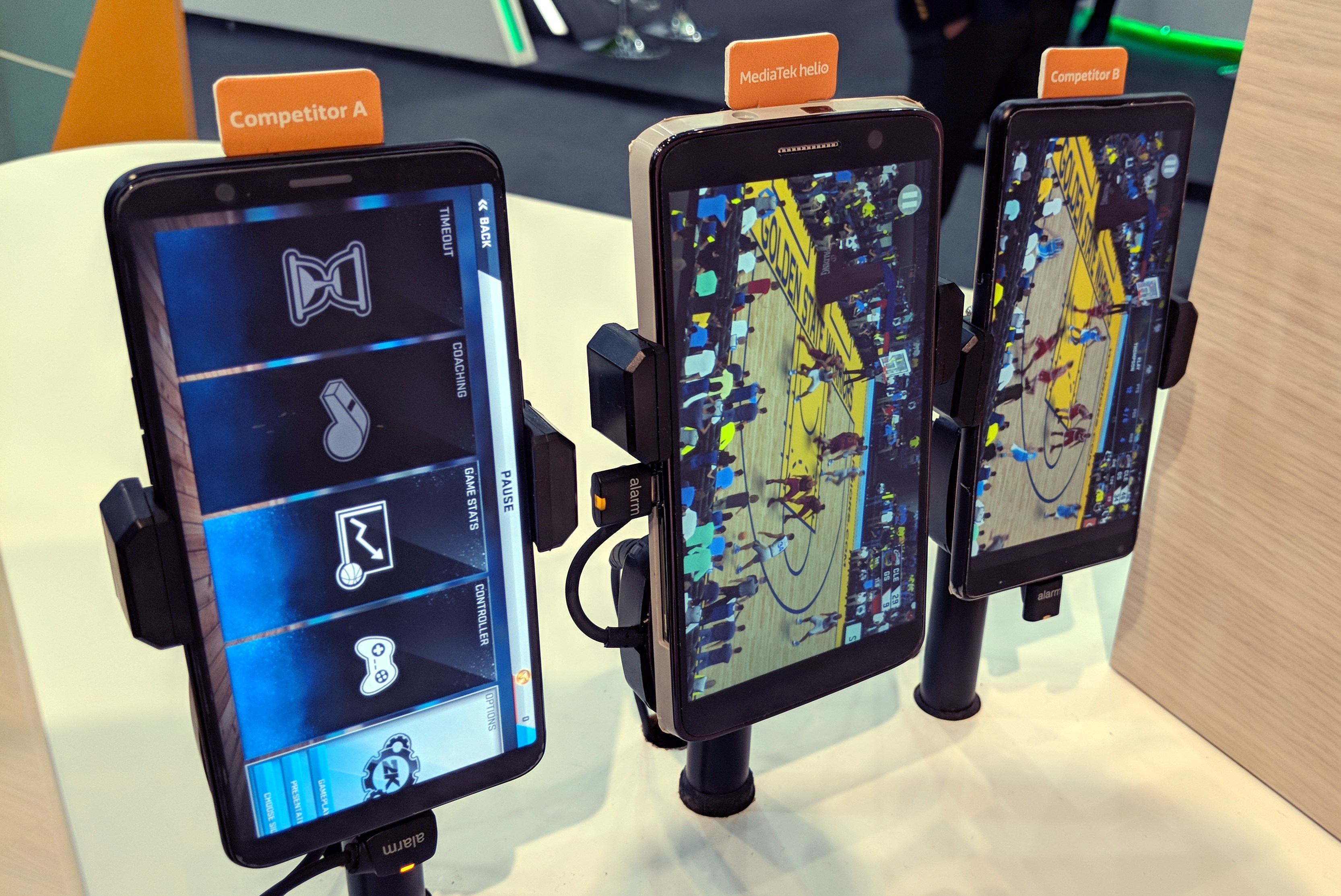
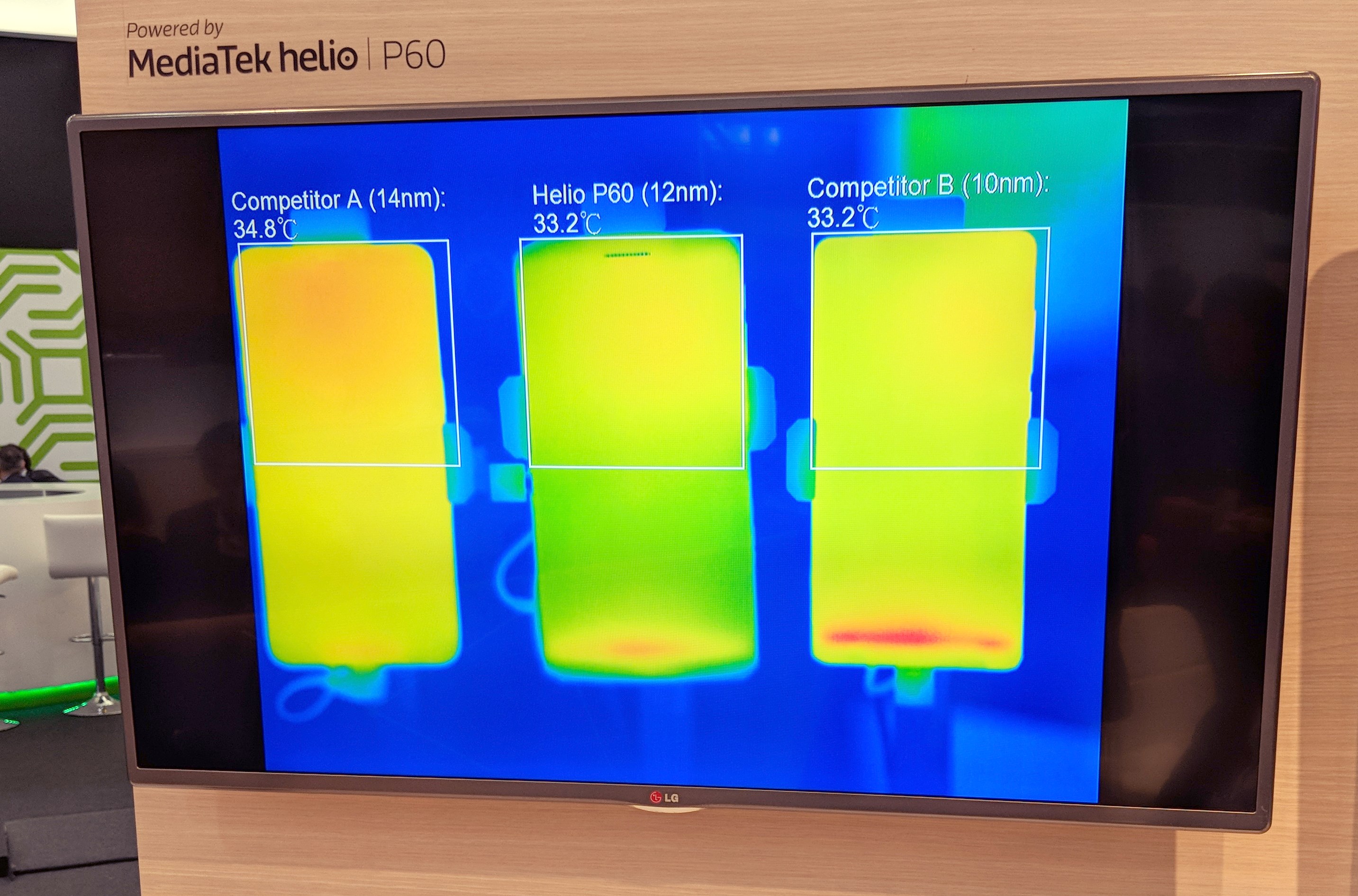
Snapdragon 660 vs Helio P60 vs Snapdragon 835 Thermal Comparison @ MWC2018
The P60 is the first mobile SoC to come manufactured on TSMC’s new 12nm 12FFC process node. 12FFC is a shrink of 16FFC and uses the same tools – it’s a cost effective alternative to the more expensive 10FF process which requires quad-patterning. While 12FFC does not quite achieve the die size reduction that 10FF would, it’s extremely competitive in terms of power characteristics and reaches near the same efficiency. I asked MediaTek about the company process roadmap plan and they will focus exclusively on 12FFC for 2018 and have no plans for further 10nm silicon. The next generation will jump directly to 7nm in mid 2019 (after other vendors) when mass production will have reached mature and cost-effective levels.
The P60 is the first SoC to bring dedicated neural network accelerators into the mid-range. MediaTek’s denomination for such IP is APU (AI Processing Unit) so that’s yet another term added to the varied basket of abbreviations from different companies. MediaTek wouldn’t disclose the IP provider but say’s it’s a dual-core implementation offering 2x140GMACs. MediaTek will offer a custom software stack called NeuroPilot which will be compatible with Google’s NN API and frameworks such as TensorFlow, TF Lite, Caffe and Caffe2.
The modem subsystem remains the same as on the Helio P30 – it supports LTE up to Category 7 with 3x20MHz CA and 300Mbps download speeds and Category 13 with 2x20MHz CA for up to 150Mbps upload speeds.
The Helio P60 is in production now and we should see consumer smartphones with the chipset available starting early Q2 2018.


74 Comments
View All Comments
ZolaIII - Friday, March 2, 2018 - link
Yup Mali T880 MP2 @ 900 MHz with DDR4 almost catches A506 @ 650 MHz with DDR 3. Take a good look what A509 (which is the same A506) archives @ 850 MHz pared with XDDR 4. To simplify the things up T880 @ 800 MHz MP4 on X20 is about as equal to A510 @ 650 MHz on S65x. So G72 MP3 @ 800 MHz is around the same performance as T880 MP4 on X20 and it will match A509 still being behind A512. Difference becomes bigger in real use when MALI throttle down while Adreno continues to pump. Still G72 is the latest MALI generation while Adreno 5xx is two + years old. Adreno 6th generation is emerging & it only makes gap wider.Plumplum - Saturday, March 10, 2018 - link
On modern fonction like Tesselation, Mali is even far better...On this Task, Mali>Adreno>powervr
For exemple, gfxbench doesn't test Tesselation on iPhone!
Give credits to 3d benchmarks is dangerous. Most time, the rendered scene in them doesn't represent well what a real game is.
A benchmark is a free software...who pays the developpers?
Nowadays, mid-range soc add Big cores.
On my opinion, buying 845 instead of 660 or P60 is useless
Benchmarks are there to give to some reasons!
Results in benchmarks oversize the importance of texturing and the difference between high-end and mid-range.
It sometime leads to strange results :
Mali 450mp6 is better than Mali T760mp2 on many benchmarks...most games run far far better on T760
ZolaIII - Sunday, March 11, 2018 - link
I give credit to sole 3D Mark regarding GPU benchmarks. You don't know what property Apple api includes support for nor is it tested or not. Most really good benchmarks aren't neither free for more precise use nor open sourced. They actually cost a lot.Your opinion isn't valid. Sure the difference in CPU in similar capable (same amount of same type of core's) is minimal & midrange SoC's even win when it comes to efficiency as aren't clocked insanely high & are made on high end manufacturing process and in real usage difference is neglectable. So if you don't play games your opinion stands. But on the other hand GPU is the biggest portion of the SoC, considerably bigger even on entry lv midrange SoC's that have let's say Mali T720 MP2. As its much bigger it also adds most of the SoC cost so in comparison the A512 on the S660 is only half size of the A540 on the S835 so the S835 costs 40% more. Still S512 is bigger than let's say Mali G72 MP4. Mali 4xx series is very old and support only EGLS 2. While Mali 450 MP6 will in fact be some 20% faster (in EGLS 2 only) than T760 MP2 its also 35~40% bigger and extremely power inefficient when a
ZolaIII - Sunday, March 11, 2018 - link
Mali 450 emulates EGLS 3.0 it became much slower in doing so that T760 that supports it nativity & most present game's use EGLS 3.0.Plumplum - Sunday, March 11, 2018 - link
It's the case even with opengl2.0The reason is that 450mp6 has heavy texturing capabilities and a big weakness with geometry...
As many benchmark mostly test texturing, the weakness doesn't appear...
...but it appears in game
ZolaIII - Monday, March 12, 2018 - link
Ok hire is contra example old San Andreas will work perfectly fine on Mali 4xx MP4 wile it will work terribly bad on Adreno 305 - 306 - 308. But it's a lonely one. After all it is mostly about poligon & texture count GPU can pump while it's easier & cheaper to improve on textures. The last generation of both Power VR and Adreno both significantly improved on texture engine & result is 30 to 50% increase in performance. Adreno has a leading ALU performance which isn't put to any good use thanks to (bad) drivers & the fact how it ain't actually needed all that much regarding actual gaming but it's much more limited to memory bandwidth & texturing capability.Plumplum - Sunday, March 11, 2018 - link
I don't since I saw a 3D benchmark that says Tegra 3's GPU was far better than Mali400mp4 and one other says exactly the opposite!3D mark is the one I prefer too!
It separates :
- texturing
- geometry
- CPU usage for physic
Others tests mostly texturing and badly represents what a game is.
They pretend flagship's GPU are 200% better than mid-range.
In game, that's nearly never the case!
P60 (or SD660)'s GPU is more than enough to run nearly all games during the life of the devices...
845 will be useless...
About tesselation on Powervr, we know that they're bad due to other soc that use them (mt8176, X30)...
We don't know about the last one
ZolaIII - Monday, March 12, 2018 - link
The benchmark results actually are accurate representative of what you get. So A540 is 2x size and 2x memory bandwidth of the A512 so it's accurately 2x performance. Games on Android do limit the frame rate to preserve battery & I know just couple game's that will give you an option to control this. Xenowerk is a prime example of options done right so you can choose the graphics lv along with 30 or 60 FPS limit. G72 MP3 on the MTK P60 (or A509 regarding performance & not throttling) will be far from enough for running all games & it will throttle (we will see how significantly), A512 on the other hand will still give 50% more performance & won't throttle but even that is either bare minimum or not sufficient enough for some titles (Dolphine emulator, Talos Principle, GOF3 to name a couple of those). A510 even with Vulkan front end in PPSSPP has a difficult time running some of more advanced game's even at 720p. Still only dumb people make game's that won't work properly on 92% of the device's when you took A512 as a base or 80~83% when you took A510, G72 MP3 or A509 as a base, but still important on the GPU front are badly needed especially in the midrange segment that actually does drive entertainment (gaming) industry base point.Plumplum - Tuesday, March 13, 2018 - link
You say it : 2x size, 2x bandwidth...to apply texture and fit to benchmarks.Comparing 509 and 510 isn't a good Idea when talking about throttling...510 use 28nm process, 509 use 14nm
Throttling is heavier on high end!
You can use gfxbench and compare Manhattan 3.1 on-screen and Manhattan long term performances.
On Mi note 3's Adreno 512 : 14.7/14.6 no throttling
On Mi 6's Adreno 540 : 35.8/28.2 throttling
On some other high-end like Galaxy S7, throttling can reach 50%...even on Real racing 3 that renders scenes in 1080, kirin's maliT880mp4 becomes faster than exynos's T880mp12!!!! Real life test!
Gfxbench's long term test isn't perfect as it doesn't saturate CPU at the same time.
Due to 28nm process 650/652 has an horrible CPU throttling, it impacts the whole soc and it's Adreno...running emulator that use both CPU and GPU kills 650/652 performances
ZolaIII - Friday, March 2, 2018 - link
Well I used TSMC own reference to it's own lithography processes, 12nm 12 mask layers, 14~16nm 14~16 mask layers. It's pretty much simple math even disregarding used rooting libs & cetera. GF statement is on their own calculations and even FD-SOI wafer costs 2x more the mask layer reduction to 8 makes it more than up for it. Still more than obvious advantages are; RF & mixed RF usability and potential of integration of all analogue, digital components on the same single package (with FinFET you can only do digital while RF remains on planar bulk & separate package[s]), back & forward biasing that gives you ability to adjust voltage (0.4V, 0.8V & beyond) & performance targets along with naturally power consumption in the flight, the rooting cost all together with less layers and compatibility tools is half of FinFET one & speed of getting job done and time to market is 50% faster (conservatively compared to simplest/cheapest 12nm 12 layers TSMC FinFET one). All faunderis use base element cell blocks for calculations and comparison but that even it's not wrong nor cheating in any way doesn't give complete final pictures as for instance base transistor cell block on one process can be bigger than competition one but base SRAM cell is smaller...Other vendors aren't so cheap basterd's so they put more GPU clusters at lower speed or better say Samsung does, HiSilicon is just a tad better than MTK regarding this & still the Samsung best effort is 2x less power efficient than Adreno. The Imagination teach did some catching but QC responded equally (also rising texture unit limit [Gx8xxx - A6XX]) pretty much zeroing that. Still me by now we will see a better competition on mobile GPU front after Chinese consortium both Imaginations GPU business.