JEDEC Publishes UFS 3.0 Spec: Up to 2.9 GB/s, Lower Voltage, New Features
by Anton Shilov on January 31, 2018 11:00 AM EST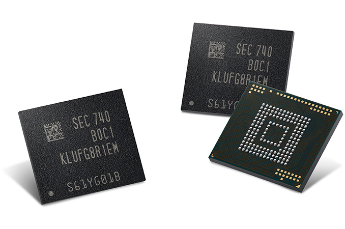
JEDEC this week published their UFS 3.0 specification, which is intended to bring numerous performance, power and feature set-related improvements to the standard. The version 3.0 of the spec doubles the per-lane performance of an eUFS device to 11.6 Gbps, which increases the peak data transfer rate of a storage device to 23.2 Gbps. At the same time, the new standard introduces a 2.5 V VCC power supply mode that enables lower power consumption and support for the latest types of NAND. Finally, the UFS 3.0 spec contains features designed specifically for automotive applications that enable standard support for extended temperature ranges as well as “refresh” operation to boost reliability.
One of the key improvements of the UFS 3.0 (JESD220D) specification is the usage of MIPI's M-PHY 4.1 physical layer as well as the recently released MIPI UniPro 1.8 protocol to form the interconnect layer (IL). The new IL supports data rates of up to 11.6 Gbps (HS-Gear4) per lane as well as QoS features to enable a more reliable link through monitoring and training of the communication channel. All UFS 3.0-compatible devices are required to support HS-G4 (11.6 Gbps) and HS-G3 (5.8 Gbps), which means that they all will be faster than UFS 2.0/2.1-compliant devices that do not necessarily support HS-G3. UFS 3.0 storage devices will continue to feature up to two full-duplex lanes, which means a theoretical maximum bandwidth of up to 23.2 Gbps (2.9 GB/s) when HS-G4 is used. The MIPI M-PHY 4.1 standard continues to use 8b10b line encoding, so accounting for the encoding overhead, the actual achievable bandwidth by an embedded UFS device will be considerably lower than the theoretical one — 15 Gbps (1.875 GB/s) is something that is reasonable to expect.
The upcoming eUFS 3.0 storage devices will require three different power rails: 1.2 V for VCCQ, 1.8 V for VCCQ2, as well as 2.5 V/3.3 V for VCC. The addition of 2.5 V for VCC is to enable support for the latest and upcoming generations of NAND flash with higher bit densities (including 3D NAND with higher amounts of layers as well as 3D TLC NAND).
The UFS 3.0 standard also supports a number of features particularly suitable for the automotive industry. UFS 3.0 devices may support a native predefined low/high temperature event notification which will simplify development of UFS-based automotive applications. Extended temperature ranges (-40°C, 105°C) will be optionally supported by host controllers. Furthermore, the latter might also adopt a standard “refresh” function to extend data retention by moving data from cell to cell to keep charges at sufficient levels.
Another important innovation of the UFS 3.0 spec is enhanced support for RPMBs (replay protected memory block). The new standard supports multiple RPMBs with multiple RPMB keys. Furthermore, RPMB regions can now be configured at manufacturing, simplifying their usage for device makers.
To simplify development of UFS-based applications going forward, JEDEC also released JESD223D — a functional specification of a UFS host controller interface (UFSHCI). This spec defines features and registers that have to be supported by UFS 3.0 host controllers and enable usage of a standard driver for all applications featuring UFS 3.0-compatible storage devices.
The UFS 3.0 standard greatly speeds up performance and capacity of storage subsystems inside smartphones, tablets, media players, VR headsets, automotive and other applications that are going to use it. Meanwhile, it is not clear when this might happen. There is at least one company who has been offering UFS 3.0 controllers since Q2 2017, but it looks like the latest mobile SoCs from Qualcomm, HiSilicon, MediaTek and Samsung do not support the new spec. That said, expect applications based on the new standard to be released in the coming years, just not in 2018.
Related Reading:
- Toshiba Samples eUFS Devices for Vehicles: Extended Temps & Reliability Features
- Samsung Starts Production of 512 GB UFS NAND Flash Memory: 64-Layer V-NAND, 860 MB/s Reads
- Toshiba Samples New UFS 2.1 NAND: Up to 900 MB/s Reads For 2018 Smartphones
- Samsung Rolls Out Its First UFS Cards: SSD Performance in Card Form-Factor
- Samsung Announces 256GB UFS Embedded Storage Solution
- Samsung Announces 128GB UFS Storage For Smartphones
Source: JEDEC


18 Comments
View All Comments
canewiliamsan - Friday, March 9, 2018 - link
Open Company in Dubai Thanks a lot for the post. It has helped me get some nice ideas. I hope I will see some really good result soon. https://www.uaefreezone.xyz/amanda - Friday, March 16, 2018 - link
thats really better to enhance the performance and overall feature of ufs.. https://professaywriters.com/amanda077 - Thursday, May 10, 2018 - link
Great info.. I think cost is not a matte if the power consumption feature is accurate.. https://professaywriters.com/abdrahim - Sunday, April 21, 2019 - link
excellent post thank from algeriawe need more feature in the future
https://ipfinder.io/
Danielperez123 - Tuesday, April 30, 2019 - link
So far this is very informative blog that I've read, Thanks for giving your effort posting this. looking forward for more update. Nice! https://www.rivalry.com/hassanshah - Wednesday, May 22, 2019 - link
Without question that the person will face 3 to 4 legal situations annually. In reality, 50% of most households use a pressing legitimate situation today. Yet, the common attorney fees around $300 hourly, which forces many individuals to have to produce a choice among eating and also legal aid. It's simply no wonder why a lot of people find that cheaper to be able to just get cheated rather than head to an legal professional, but you can find options accessible. <a href="http://www.legalhelps.ca">legalhelps.ca<...malinaxxx - Thursday, January 23, 2020 - link
Is there a reason smartphones don't just use pciexpress?https://www.elitetorrentt.com/
christinepbaynec - Wednesday, April 13, 2022 - link
A paediatrician provides medical care for children who are ill and also provide preventive health services for healthy children. https://doctorshospital.in/paediatrics