NVIDIA Volta Unveiled: GV100 GPU and Tesla V100 Accelerator Announced
by Ryan Smith on May 10, 2017 5:00 PM EST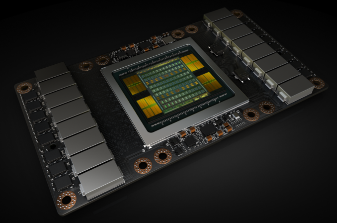
Today at their annual GPU Technology Conference keynote, NVIDIA's CEO Jen-Hsun Huang announced the company's first Volta GPU and Volta products. Taking aim at the very high end of the compute market with their first products, NVIDIA has laid out a very aggressive technology delivery schedule in order to bring about another major leap in GPU deep learning performance.
As a quick history lesson, NVIDIA first unveiled the Volta architecture name all the way back in 2013. What eventually happened with their architectures wasn’t what was originally announced – Maxwell and Volta became Maxwell, Pascal, and Volta – but Volta is the last GPU architecture on NVIDIA’s current public roadmap. Until now, all we’ve known about Volta is that it existed; NVIDIA has opted to focus on what’s directly in front of them (e.g. Pascal), one generation at a time.
So let’s talk Volta. For their first Volta products, NVIDIA is following a very similar path as they did with Pascal last year. Which is to say that they are kicking off their public campaign and product stack with a focus on business, HPC, and deep learning, rather than consumer GPUs. Volta is a full GPU architecture for both compute and graphics, but today’s announcements are all about the former. So the features unveiled today and as part of the first Volta GPU are all compute-centric.
NVIDIA’s first Volta GPU then is the aptly named GV100. The successor to the Pascal GP100, this is NVIDIA’s flagship GPU for compute, designed to drive the next generation of Tesla products.
| NVIDIA GPU Specification Comparison | |||||
| GV100 | GP100 | GK110 | |||
| CUDA Cores | 5376 | 3840 | 2880 | ||
| Tensor Cores | 672 | N/A | N/A | ||
| SMs | 84 | 60 | 15 | ||
| CUDA Cores/SM | 64 | 64 | 192 | ||
| Tensor Cores/SM | 8 | N/A | N/A | ||
| Texture Units | 336 | 240 | 240 | ||
| Memory | HBM2 | HBM2 | GDDR5 | ||
| Memory Bus Width | 4096-bit | 4096-bit | 384-bit | ||
| Shared Memory | 128KB, Configurable | 24KB L1, 64KB Shared | 48KB | ||
| L2 Cache | 6MB | 4MB | 1.5MB | ||
| Half Precision | 2:1 (Vec2) | 2:1 (Vec2) | 1:1 | ||
| Double Precision | 1:2 | 1:2 | 1:3 | ||
| Die Size | 815mm2 | 610mm2 | 552mm2 | ||
| Transistor Count | 21.1B | 15.3B | 7.1B | ||
| TDP | 300W | 300W | 235W | ||
| Manufacturing Process | TSMC 12nm FFN | TSMC 16nm FinFET | TSMC 28nm | ||
| Architecture | Volta | Pascal | Kepler | ||
Before we kick things off, one thing to make clear here - and this is something that I'll get into much greater detail when NVIDIA releases enough material for a proper deep dive - is that Volta is a brand new architecture for NVIDIA in almost every sense of the word. While the internal organization is the same much of the time, it's not Pascal at 12nm with new cores (Tensor Cores). Rather it's a significantly different architecture in terms of thread execution, thread scheduling, core layout, memory controllers, ISA, and more. And these are just the things NVIDIA is willing to talk about, never mind the ample secrets they still keep. So while I can only scratch the surface for today's reveal and will be focusing on basic throughput, Volta has a great deal going on under the hood to get to in the coming weeks.
But starting with the raw specficiations, the GV100 is something I can honestly say is a audacious GPU, an adjective I’ve never had a need to attach to any other GPU in the last 10 years. In terms of die size and transistor count, NVIDIA is genuinely building the biggest GPU they can get away with: 21.1 billion transistors, at a massive 815mm2, built on TSMC’s still green 12nm “FFN” process (the ‘n’ stands for NVIDIA; it’s a customized higher perf version of 12nm for NVIDIA).
To put this in perspective, NVIDIA’s previous record holder for GPU size was GP100 at 610mm2. So GV100, besides being on a newer generation process, is a full 33% larger. In fact NVIDIA has gone right to the reticle size of TSMC’s process; GV100 is as big a GPU as the fab can build. Now NVIDIA is not a stranger with reticle sizes, as GM200 happened to do the same thing with TSMC’s 28nm process, but at only 601mm2, GV100 is much larger still.
Now why the focus on die size first and foremost? At a high level, die size correlates well with performance. But more significantly, this is a very visible flag about how NVIDIA is pushing the envelope. The company is not discussing chip yields at this time, but such a large chip is going to yield very poorly, especially on the new 12nm FFN process. NVIDIA is going to be sacrificing a lot of silicon for a relatively small number of good chips, just so that they can sell them to eager customers who are going to pay better than $15K/chip. This is how badly NVIDIA’s customers want more powerful GPUs, and how hard NVIDIA is going to push the limits of modern fab technology to deliver it.
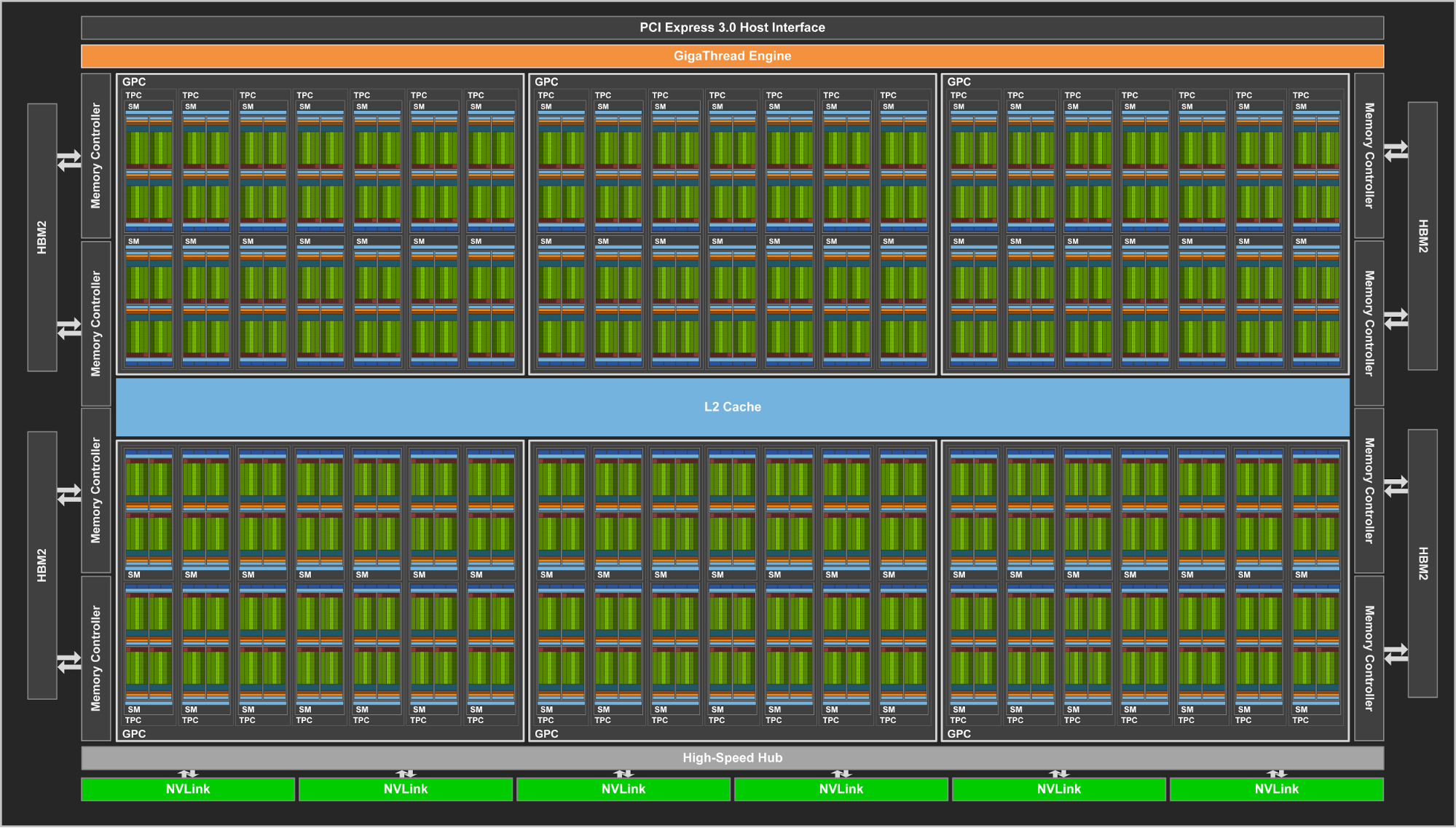
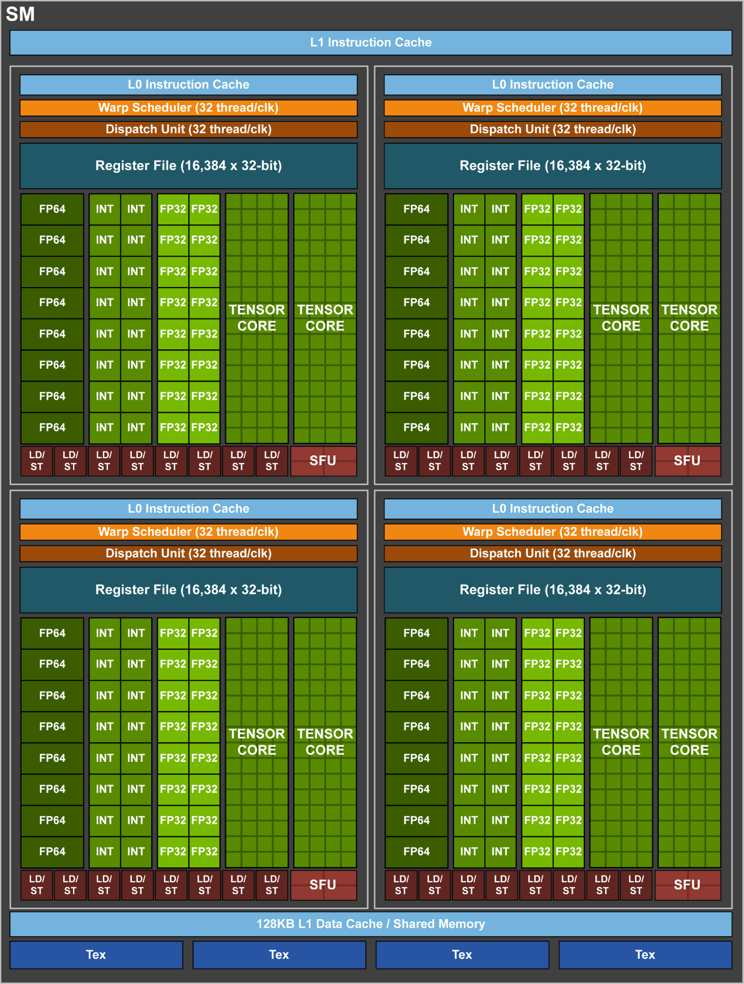
The chip’s absurd size aside, GV100 promises to be powerful. The chip contains 84 SMs – as this is a compute product, each SM is 64 CUDA cores in size – making for a total of 5376 FP32 CUDA cores. Joining those FP32 cores are 2688 FP64 CUDA cores (meaning NV is maintaining their 1:2 FP64 ratio), but also a new core that NVIDIA is calling the Tensor Core.
Tensor Cores are a new type of core for Volta that can, at a high level, be thought of as a more rigid, less flexible (but still programmable) core geared specifically for Tensor deep learning operations. These cores are essentially a mass collection of ALUs for performing 4x4 Matrix operations; specifically a fused multiply add (A*B+C), multiplying two 4x4 FP16 matrices together, and then adding that result to an FP16 or FP32 4x4 matrix to generate a final 4x4 FP32 matrix.
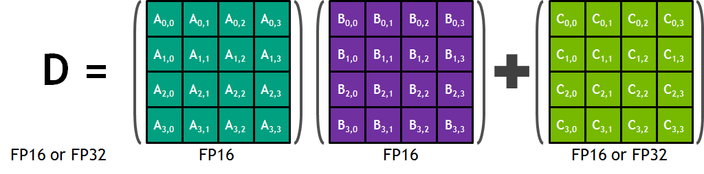
The significance of these cores are that by performing a massive matrix-matrix multiplication operation in one unit, NVIDIA can achieve a much higher number of FLOPS for this one operation. A single Tensor Core performs the equivalent of 64 FMA operations per clock (for 128 FLOPS total), and with 8 such cores per SM, 1024 FLOPS per clock per SM. By comparison, even with pure FP16 operations, the standard CUDA cores in an SM only generate 256 FLOPS per clock. So in scenarios where these cores can be used, NV is slated to be able to deliver 4x the performance versus Pascal.
Now there are a bunch of unknowns here, including how flexible these cores are, and how much die space that they take up versus FP32 CUDA cores. But at a high level, this is looking like a relatively rigid core, which would make it very die-space efficient. By lumping together so many ALUs within a single core and without duplicating their control logic or other supporting hardware, the percentage of transistors in a core dedicated to ALUs is higher than on a standard CUDA core. The cost is flexibility, as the hardware to enable flexibility takes up space. So this is a very conscious tradeoff on NVIDIA’s part between flexibility and total throughput.
Continuing down the spec list, each SM contains 4 texture units, the same number as with the GP100. Joining those texture units is yet another rework of NVIDIA’s L1 cache/shared memory architecture. Whereas GP100 had a 24KB L1/Texture cache and 64KB shared memory per SM, on GV100 it’s now a 128KB of L1 data cache/shared memory per SM, with the precise L1/shared memory split being configurable. Besides unifying these caches, this means there’s more cache/memory overall, 40KB more per SM. On the other hand, the register file remains unchanged at 256KB of registers (4x16K 32-bit registers) per SM.
At a higher level, the 84 SMs are organized 2 to a TPC, just as with GP100, giving us a 42 TPC count. These TPCs are in turn organized 7 to a GPC, and then 6 GPCs. Feeding the beast is once again HBM2, with NVIDIA using 4 stacks of it like GP100. It’s interesting to note here that while memory clocks have only increased by 25% for the respective Tesla SKUs, NVIDIA is claiming a 50% increase in effective memory bandwidth due to a combination of that and better memory efficiency. Meanwhile the L2 cache system between the memory and GPCs has also been enhanced; there’s now 768KB of L2 cache per ROP/memory partition, versus 512KB on GP100. This means L2 cache for the whole chip now stands at 6MB.
Going to a higher level still, Volta also implements a newer version of NVLink. This is the previously announced NVLink 2, and along with greater link bandwidth – up from 20GB/sec bidirectional to 25GB/sec bidirectional – there are now 6 NVLinks per GPU for GV100, 2 more than on GP100. Critically, NVLInk 2 also introduces cache coherency allowing the GPUs to be cache coherent with CPUs. Expect to see this play a big part in the eventual Power 9 + Volta systems.
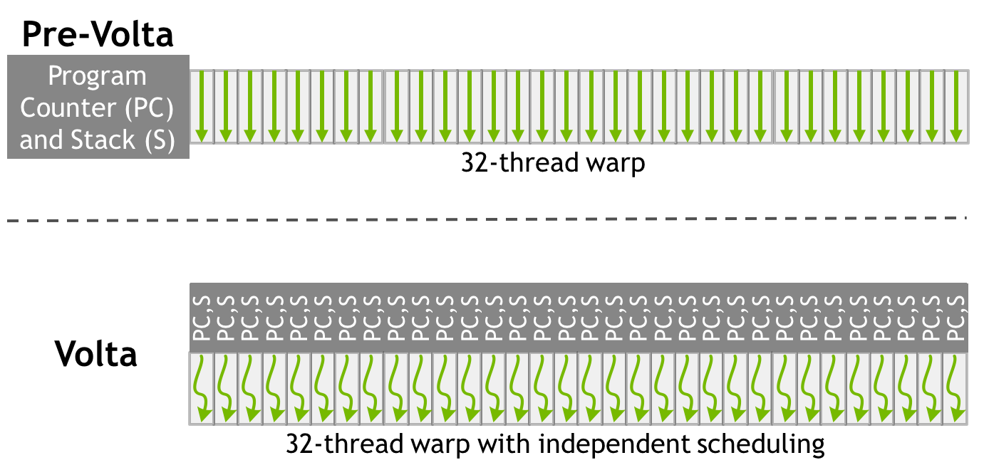
Finally, while the full details on this will have to wait until later, NVIDIA has also unveiled that they’ve made a pretty significant change to how SIMT works for Volta. The individual CUDA cores within a 32-thread warp now have a limited degree of autonomy; threads can now be synchronized at a fine-grain level, and while the SIMT paradigm is still alive and well, it means greater overall efficiency. Importantly, individual threads can now yield, and then be rescheduled together. This also means that a limited amount of scheduling hardware is back in NV’s GPUs.
Overall, GV100 is a 3 billion dollar R&D project for NVIDIA, their largest project to date for their largest GPU to date. NV is expecting the first GV100 products to start shipping in Q3 of this year and they won’t be cheap – on the order of $18K per GPU for a DGX system – however for those customers with deep pockets and who will essentially pay NVIDIA to eat the risk of producing such a large GPU, this will be the most powerful GPU released yet.
Tesla V100
The first product to use the GV100 GPU is in turn the aptly named Tesla V100. Like its P100 predecessor, this is a not-quite-fully-enabled GV100 configuration. Overall, only 80 of 84 SMs are enabled for yield reasons.
| NVIDIA Tesla Family Specification Comparison | ||||||
| Tesla V100 | Tesla P100 | Tesla K40 | Tesla M40 | |||
| Stream Processors | 5120 | 3584 | 2880 | 3072 | ||
| Core Clock | ? | 1328MHz | 745MHz | 948MHz | ||
| Boost Clock(s) | 1455MHz | 1480MHz | 810MHz, 875MHz | 1114MHz | ||
| Memory Clock | 1.75Gbps HBM2 | 1.4Gbps HBM2 | 6Gbps GDDR5 | 6Gbps GDDR5 | ||
| Memory Bus Width | 4096-bit | 4096-bit | 384-bit | 384-bit | ||
| Memory Bandwidth | 900GB/sec | 720GB/sec | 288GB/sec | 288GB/sec | ||
| VRAM | 16GB | 16GB | 12GB | 12GB | ||
| Half Precision | 30 TFLOPS | 21.2 TFLOPS | 4.29 TFLOPS | 6.8 TFLOPS | ||
| Single Precision | 15 TFLOPS | 10.6 TFLOPS | 4.29 TFLOPS | 6.8 TFLOPS | ||
| Double Precision | 7.5 TFLOPS (1/2 rate) |
5.3 TFLOPS (1/2 rate) |
1.43 TFLOPS (1/3 rate) |
213 GFLOPS (1/32 rate) |
||
| GPU | GV100 (815mm2) |
GP100 (610mm2) |
GK110B | GM200 | ||
| Transistor Count | 21B | 15.3B | 7.1B | 8B | ||
| TDP | 300W | 300W | 235W | 250W | ||
| Cooling | N/A | N/A | Active/Passive | Passive | ||
| Manufacturing Process | TSMC 12nm FFN | TSMC 16nm FinFET | TSMC 28nm | TSMC 28nm | ||
| Architecture | Volta | Pascal | Kepler | Maxwell 2 | ||
By the numbers, Tesla V100 is slated to provide 15 TFLOPS of FP32 performance, 30 TFLOPS FP16, 7.5 TFLOPS FP64, and a whopping 120 TFLOPS of dedicated Tensor operations. With a peak clockspeed of 1455MHz, this marks a 42% increase in theoretical FLOPS for the CUDA cores at all size. Whereas coming from Pascal, for Tensor operations the gains will be closer to 6-12x, depending on the operation precision.
The Tesla V100 will be paired with 16GB of HBM2. At this time no one is producing an 8-Hi HBM2 stack, so NVIDIA cannot expand their memory capacity at 4 stacks. However the memory clockspeed has improved by 25% over Tesla P100, from 1.4Gbps to 1.75Gbps.
Also like the Tesla P100, NVIDIA is using a mezzanine card. They have not shown the new connector – expect it to have more pins to account for the additional NVLinks – but the overall size is similar. NVIDIA calls this the SXM2 form factor.
In terms of power consumption, Tesla V100 will have a TDP of 300W, like its predecessor. NVIDIA notes that power efficiency of V100 is higher than P100, though it will be interesting to see just where this stands, and how often the card actually power throttles.
The first product to ship with Tesla V100 will be the NVIDIA DGX-1V, the Volta version of their DGX server. Similar to their Pascal launch, starting with DGX sales allows NVIDIA to sell 8 GPUs in one go, and for a premium at that. A DGX-1V will set you back a cool $149,000. The payoff? It ships in Q3, whereas OEM P100 designs won’t be available until Q4.
Finally, along with the mezzanine version, NVIDIA has also announced two PCIe versions of the V100. The first is a full size 250W card, analogous to the PCIe Tesla P100. The second is a smaller full height half length PCIe card, which for now is being dubbed the “Tesla V100 for Hyperscale Inference”. This is a 150W card, and is specifically meant for dense configurations in datacenter inference servers. The specifications have not been published yet, but given that it has half the TDP of the mezzanine card, it’s a safe bet that it’s clocked lower and features more disabled SMs than the full fat version.


179 Comments
View All Comments
theuglyman0war - Sunday, May 14, 2017 - link
The only gaming I have done is stereoscopic since 2010 and I won't but a monitor that doesn't support 3Dvision. Between Helix 3DMigato and WSGF/Hayden's Flawless 3d Surround community solutions... I usually have no problems. The industry and naysayers confuse saturation with obsolescence. Stereoscopic markets between Theater VR and Gaming will be a multi Billion dollar industry as long as we have two eyes.CiccioB - Thursday, May 11, 2017 - link
Sorry to disturb your dreams, but AMD has inferior technology with respect to nvidia.I do not knwo how you calculate "not being inferior" but nvidias technology allows to use less energy to do the same work on GPGPU and also less silicon for 3D pipeline.
Combined nvidia offers much better products that AMD can counte attack only producing much beefed and energy hungry GPUs making their upper line match with nvidia lower line.
Margins are then quite different.
And those margins are those that make AMD "poor". This has been for year now. GCN has annihilated any AMD advantage (with Terascale at least they could make smaller chips).
Now they are behind under all point of view: size, energy and performance.
How can you say AMD is not inferior is just a mere symptom of being blinded by red glasses.
Again sorry, but reality is different.
BTW, this is a beast that has not a single competition from any other HPC card producer. Vega won't touch the heels of this GPU. It just means nvidia needs to cut this down to bare minimum as they did with GP102 and have a winning GPU that is going to crush Vega without having to use expensive HBM2 (another reason of different margins.. one uses optimized technology that makes maximum use of bandwidth, the other just feeds as much bandwidth as possible with gargantuan costs).
I may say that when nvidia will release Volta it will be a complete generation ahead of AMD which will have something to fight back only with Navi, a year later. Possibly, too few too late.
vladx - Thursday, May 11, 2017 - link
Damn CiccioB, you're a savageddriver - Thursday, May 11, 2017 - link
Nvidia has enough money to produce different chip versions of the same family - amd does not.Nvidia cuts everything that is non essential to games to produce a castrated chip, which obviously, will consume less power, since it is much less capable. They have been cutting literally every corner, which should be obvious even to a fanboy like you, considering that their legacy title performance advantage is not reflected into DX12 and Vulkan titles, because the hardware isn't really "next gen" capable for the sake of transistor savings.
Amd meanwhile is forced to use the same chip for both mainstream and professional products, thus the chip has to have some redundancies, which hurt its power efficiency in tasks which do not call for such features, because they don't have the resources to produce numerous flavors of every chip. Which is why amd is also forced to make more future proof designs, that actually have performance benefits from running DX12 and Vulkan titles rather than the performance degradation exhibited by nvidia's GPUs.
Amd is also making this transition, however due to the shortage of funds, far more slowly. They now have different chip flavors for their high end workstation GPUs, whereas couple of years back it was still the same chip, just different drivers. Which is why Amd GPUS had tremendously better FP64 rates, like 1/2 or 1/3 of FP32, whereas nvidia has gutted that a long time ago, and it should go without saying, but I'll say it nonetheless, since it doesn't look like reasoning is not your strong point, if you sack FP64 throughput to 1/32 you will obviously save on some power.
Another big power saver for nvidia is tile based rendering, the patent of which expired recently. Amd will also incorporate it in Vega, but again, due to the lack of funds, it took much longer to implement than it did nvidia.
Amd can easily scale its designs up to match that thing, had it had the resources to make it and market to sell it, but they don't have either. Nvidia's advantage is entirely logistical. Their technological superiority only exists in the wet dreams of fanboys like you.
Amd being "poor" doesn't have anything to do with the quality of its products, amd was poor even when its products had a pronounced edge over the competition
"How can you say AMD is not inferior is just a mere symptom of being blinded by red glasses."
Nah, I just understand the technology, the industry and the market, unlike you, who only understands marketing hype.
Strunf - Thursday, May 11, 2017 - link
AMD doesn't have the money to make different flavors of the same chip? what you can the RX 480, RX470 and RX460 ? and now the RX580, 570 and 560. Different flavors cost little to nothing, easy peasy to disable parts of a chip, tapping out optimized versions costs more on R&D but also gives bigger returns (less waste). And what about the FURY thing sure no money for some stuff but to spend money on experimental HBM products they seem to have...Tile based rendering a patent? it's over 20 years old technology, and why would it be worthy of a patent it's just a division of the image into smaller blocks.
Well being poor didn't stop AMD from buying ATI... AMD has money (big investors behind) they just made bad choices.
fanofanand - Thursday, May 11, 2017 - link
Your lack of understanding is stunning! By different chips, he means compute vs graphics. If tile based rendering sucked then why is Nvidia now using it (now that the patent has expired). The 480/470/460 are NOT different chips, they are the same chip with some of the SM's disabled. Just stop commenting and start reading. Learn a bit more before you start spouting off. You made me defend ddriver which is not something I'm comfortable with.CiccioB - Thursday, May 11, 2017 - link
You should learn as well. Fiji was a complete new architecture with respect to previous GCN based GPUs, a project that costed a lot of money. The simple justification of that wasted amount of money was the use of new HBM memory that did not brought any advantage.BTW, Fiji was a compute chip on the contrary, that is AMD decided to create a big chip only for the consumer market (no DP capacity). So they have made distinction between consumer and computing market, but they get it wrong because they prefer to follow other priorities (trying to get at least a chip ahead of the competition after so many years behind). They failed nonetheless.
Another bunch of money thrown away when they could have been used more cleverly for optimizing Polaris, which could have been more efficient and so they could also make a larger chip to really fight against GP104.
The situation of the actual AMD architecture is not happened by chance suddenly in a night. It is the evolution of a series of choices AMD has brought forward during these years. If the situation is that they cannot afford to have two really different architecture is their responsability.
They started thinking that combining FP32 ALU to get FP64 one was a clever move to save die space. But that had other drawbacks that they thought were not so important.
Unfortunately they are (mainly efficiency). Now it is not an nvidia problem if they decided to make much more efficient architectures by sacrificing die space on computing GPUs (that however are sold with premium margins that it does not matter) and so being able to offer better products on both markets.
AMD will arrive at the same strategy (it is already there to tell you the truth), but as often has happened in last 10 years, it has arrived at the same competition conclusion after that it has see it applied by others and a couple of years late.
mat9v - Thursday, May 11, 2017 - link
AMD did not fail with Fiji, it works great as pro chip, it's just that they made it with not enough ROPs for the amount of SP they included. Yes it was a serious error in the project, it does not mean that whole archi was a bust. ROPs after all are not used in professional computations. Fiji also had less then stellar amount of memory. At the time of Fiji premiere there were not "years behind Nvidia", at most 1 generation and Fury X barely lost to 980Ti while winning with standard 980. In fact 980Ti was a reaction from Nvidia to the Fury X premiere. Granted Fury was far less efficient chip then 980 family and OC was a bust there.Yup, you are right, Nvidia has much more money (valuation of AMD is about 10B $ while Nvidia is about 70B $) and is in the green so they can afford to create different designs for different markets, it's hard to tell how the design and production costs impact margins but I guess they have enough volume to justify that. It is sad day when on Amazon, first 15 places on "most units sold/popular" list occupied by Nvidia cards :( Hopefully Vega will make some inroads into client's hearts :)
CiccioB - Friday, May 12, 2017 - link
How can you say Fiji was not a fail?It could not satisfy a single point of its original intentions.
1. Win against GM200 no matter the cost:it failed despite super expensive HBM
2. Being used in professional card: it failed, 4GB of RAM is just 4 years old capacity
3. Make AMD gain some money: it failed, its cost was so high and the clever move of nvidia to place GTX980Ti to a quite low price (lower than it was really needed) just killed any AMD margin they could think they could have made on it
4. Make AMD gain experience with HBM for having an advantage with the next generation: failed, AMD did not use HBM; in any form while nvidia started using HBM2 as soon as it was available. A year and half later AMD has still nit launched a card with HBM2 memory.
What are the winning points of Fiji? Working great as a Pro chip? Where? It was even not put into a professional class card but that Pro Duo that was created just to dispose of the last Fiji chips that otherwise had to be sold for the price of a beer. And they probably sold ten of them on the entire planet.
Fiji has been the most disappointing GPU after R600. So many costs, so many expectations, so little returned. Saying that it did great against 980 is like saying that Hawaii is a great GPU because it manage to win against a 750Ti. You can compare it what whatever you want and be happy it is faster that it, but the lower the comparison the lower the value of the GPU.
CiccioB - Thursday, May 11, 2017 - link
With this you've just thrown the mask and show the small shallow fanboy in you.For the FP64 bit blabbing, I would just recall that both Tonga and Fiji where highly castrated under this point of view and yet Fiji + HBM could not reach GM200 performances but in few optimized situations at 4K (and had really great problems at lower resolution that even Hawaii sometimes was near to its performances) while Tonga (aka 380) was a monster (in dimensions and power consumption) against the much smaller and super efficient GM106 (aka GTX960).
Last but not least, Polaris has not FP64 capacity better than consumer Pascal and yet the 580 uses a twice energy hungry and bigger die (using a denser PP nonetheless) than the 1060 it tries to beat.
The fact that AMD has always tried to sell FP64 capabilities in consumer market (since Terascale) its all their fault, not a problem of money. It was a wrong strategy and AMD seems to have understood how stupid this was.
However it just allows them to spare few watts with respect to the immense inefficiency their architecture has.
About the DX12 performances, what are you talking about with "future proof design"? The one that gains 10% of performances using double the energy? 30% more silicon? 30% more TFLOPS to do the same work?
Are you implying that using all this extra resources to gain 10% of performances in those (few) optimized games for AMD architecture (requiring further work payed by AMD to support its "advanced tech") is a "future proof design"?
Future for when? 10 years after their release? We are beyond 2 years after DX12 launch, in a market dominated by console porting, running on AMD DX12 capable HW... still nothing really that makes DX12 overcome DX11 (ah, the low level promises of much metter performances in exchange of a much harder and costly work for the programmers).
Unfortunately for you, that still look at the reality though red glasses, in DX12 nvidia games are not let in dust like your dreams make you think. They are quite competitive. It does not require nvidia to revolutionize their architecture to gain that 10% difference. Keeping their GPUs always smaller and cheaper than the concurrent ones. And new DX11 games are stil constantly released making "the advanced AMD architecture" ridiculous.
Being stronger using more resource is not an indication of having "better technology", my dear.
On the contrary. Running an entire F1 grand prix with a Prius and arriving 1 meter head (that's enough to win) of a McLaren doesn't indicates that the two cars have the same level technology. Don't you agree? And even in the few occasions when the McLaren wins by 1 meter you can't say "huuuhuu.. what a fantastic car future proof.. we will use it for the next year as well!"
AMD is well being nvidia current architecture. You may believe what you want on FP64 (which I proved you just do not know what you are talking about), you just admitted that nvidia rasterization is superior (and AMD is going to copy it a couple of generation later like it did with nmuch of nvidia architecture when passing from Terascale to GCN), nvidia memory bandwidth usage is better (and that is witnessed by same performances GPU like GP106 and Polaris 10, or that is the same that GP104 with same bandwidth can deliver 50% more performances), you can babble whatever you have heard in some fanboy club about this useless (performance wise) asynchronous technique that just try to lower AMD architecture inefficiencies. You know Fiji is a 8.9TFLOPS GPU and GM200 5.6TFLOPS GPU, do you? Or that Polaris 10 is a 5.5TFLOPS GPU and GP106 just 4.3TFLOPS? WOW async allows this one to have 10% advantage in Vulkan based games! And 6% in DX12 games that heavily use async, that is only the 4 ones that are based on DICE engines that have been payed by AMD just to exploit all AMD architecture capacity! 10% more! With double the power usage (see 580 hyper OC 240W to have this advantage)! Incredible! How better is AMD architecture, isn't it?
Come on, you can do better than this. Just wake up and stop believing in your wet dreams where AMD is something that in reality it is not. You may have been sleeping too much to be aware that nvidia cards using smaller and cheaper components are sold for a higher price. Maybe because nvidia cards are better that AMD ones that have to be under priced to be sold in a decent number?
The poor AMD is poor because it has been selling products with ridiculous margins for years because their technology was sub par. It is doing the same today. It seems it won't be different with Vega, and you dare to say that AMD is not technologically ownd by AMD?
PUT OF THOSE RED GLASSES, PAL! Oy you won't understand anything of what is coming next as much as you have not understood why "the poor" AMD is in this position today.